Klocke Nanotechnik Micro Production Precision Manipulation and Metrology System
| Brand | Klocke Nanotechnik |
|---|---|
| Origin | Germany |
| Model | Micro Production |
| Type | Precision Nanomanipulation & 3D Coordinate Metrology Platform |
| Application Domain | Semiconductor Process Development, In-situ SEM/TEM Nanomanipulation, MEMS/NEMS Characterization, Nanofabrication Integration |
| Compliance | Designed for ISO 14644-1 Class 5 cleanroom environments |
| Positioning Resolution | Sub-nanometer (≤1 nm) in X/Y/Z |
| Force Sensing Capability | Integrated piezoresistive microforce feedback (mN range) |
| Vacuum Compatibility | Fully compatible with high-vacuum SEM/TEM chambers (10⁻⁷ mbar and below) |
| Interface | Standardized flange mounts (CF, KF, or custom) for JEOL, Zeiss, Thermo Fisher (FEI), Hitachi, TESCAN, and Raith systems |
Overview
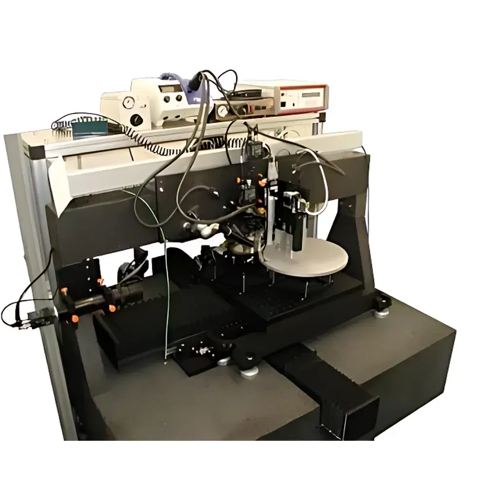
The Klocke Nanotechnik Micro Production system is a high-precision, modular nanomanipulation and metrology platform engineered for semiconductor process development, in-situ electron microscopy, and advanced micro/nanoscale fabrication. Built upon over three decades of expertise in nanoscale mechanics—dating back to Klocke Nanotechnik’s foundational work on microgrippers in 1994—the system implements closed-loop piezoelectric actuation combined with real-time force feedback and sub-nanometer spatial resolution. Its core architecture adheres to the principles of Coulomb friction compensation, thermal drift mitigation, and vacuum-stable kinematic design, enabling stable, repeatable manipulation under scanning electron microscope (SEM), transmission electron microscope (TEM), and focused ion beam (FIB) imaging conditions. Unlike generic positioning stages, the Micro Production platform integrates coordinated motion control across three orthogonal axes with synchronized force sensing—making it suitable not only for physical handling but also for quantitative mechanical property assessment (e.g., nanoindentation, tensile testing of nanowires, and probe-based electrical characterization) during live imaging.
Key Features
- Sub-1 nm open-loop positioning resolution and ≤2 nm closed-loop repeatability in all three Cartesian axes
- Integrated piezoresistive force sensor with calibrated output (range: 0.1–50 mN, resolution: 10 µN)
- Vacuum-rated construction using non-outgassing ceramics and ultra-low-magnetic stainless steel alloys
- Standardized mounting interfaces for seamless integration into JEOL JSM-6500F, Zeiss Sigma/Supra, Thermo Fisher Helios G4 UX, Hitachi SU-4800-II, TESCAN MIRA, and Raith e_LiNE platforms
- Modular tooling support: interchangeable NMG (Nano Micro Gripper) end-effectors, tungsten or Pt/Ir conductive probes, AFM-like cantilevers, and MEMS-compatible microtweezers
- Real-time synchronization with microscope image acquisition via TTL trigger and analog voltage output for correlation of position/force data with frame timestamps
Sample Compatibility & Compliance
The Micro Production system is validated for use with silicon wafers (200 mm and 300 mm), compound semiconductor substrates (GaN, SiC, InP), MEMS devices, photonic integrated circuits (PICs), and nanowire arrays. It complies with ISO 14644-1 Class 5 cleanroom operational requirements and meets material compatibility standards per SEMI F27-0204 (cleanliness of semiconductor equipment surfaces). All moving components are free of lubricants and employ ceramic-on-ceramic bearing interfaces to prevent hydrocarbon contamination in vacuum. The system supports GLP-compliant operation through audit-trail-enabled firmware logging (timestamped position, force, and status events), aligning with FDA 21 CFR Part 11 expectations for regulated R&D environments.
Software & Data Management
Control is managed via Klocke’s proprietary NanoControl Suite v4.x—a Windows-based application supporting both manual joystick-driven operation and scriptable automation (Python API included). The software provides synchronized multi-channel data acquisition (position X/Y/Z, force Fx/Fy/Fz, temperature, and external trigger signals), export in HDF5 and CSV formats, and native compatibility with MATLAB and Python-based analysis pipelines. Raw datasets include metadata compliant with FAIR principles (Findable, Accessible, Interoperable, Reusable), facilitating traceability in semiconductor process qualification workflows. Optional add-ons include automated feature tracking (for drift correction) and machine-learning-assisted grasp-point prediction for irregular microstructures.
Applications
- In-situ mechanical testing of interconnects and TSVs (through-silicon vias) inside dual-beam FIB-SEM systems
- Probe-based IV/CV characterization of nanoscale transistors and 2D material heterostructures
- Assembly and alignment of photonic waveguides and plasmonic antennas on SOI wafers
- Failure analysis of solder bumps and Cu pillars using force-controlled micro-probing
- Calibration and validation of reference artifacts for SEM-based critical dimension (CD-SEM) metrology
- Development of nanorobotic workflows for autonomous pick-and-place in advanced packaging R&D
FAQ
Is the Micro Production system compatible with cryo-SEM or cryo-TEM configurations?
Yes—custom low-temperature variants are available with liquid nitrogen cooling channels and thermal expansion-compensated kinematics for operation down to 100 K.
Can the system be retrofitted into an existing SEM chamber without chamber modification?
Standard configurations use CF-63 or CF-100 flanges; minor port adaptation may be required depending on chamber geometry—Klocke provides detailed mechanical interface drawings and installation support.
Does the force feedback module meet ASTM E2546-22 requirements for nanomechanical testing?
While not certified as a standalone test instrument, its force calibration traceability follows DIN EN ISO/IEC 17025 via DAkkS-accredited third-party labs, satisfying pre-test verification criteria outlined in ASTM E2546-22 Annex A2.
What level of electromagnetic interference (EMI) shielding does the system provide?
All electronics are housed in mu-metal-shielded enclosures meeting IEC 61000-4-3 Level 3 radiated immunity requirements, ensuring stable operation near high-power FIB columns.
Is remote operation supported for multi-site semiconductor R&D teams?
Yes—via secure TLS-encrypted VNC tunneling with role-based access control (RBAC); full audit logs are retained for ISO 9001 internal audits.


