LEI-TECH LK-CJS6300 Ultra-Deep Depth of Field Digital Microscope System
| Brand | LEI-TECH |
|---|---|
| Origin | Tianjin, China |
| Manufacturer Type | OEM Manufacturer |
| Model | LK-CJS6300 |
| Imaging Sensor | 1/1.7″ CMOS, 3840 × 2160 (4K) @ 60 fps |
| Optical Zoom Range (Configurable) | 30×–500× or 80×–6500× |
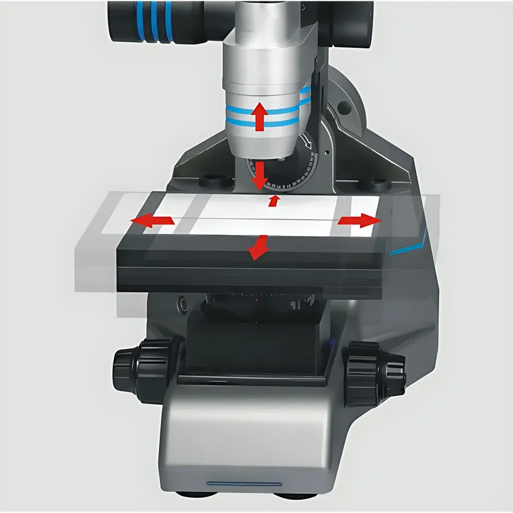
| Motorized XYZ Stage | X/Y travel 205 mm × 180 mm, resolution 1 µm |
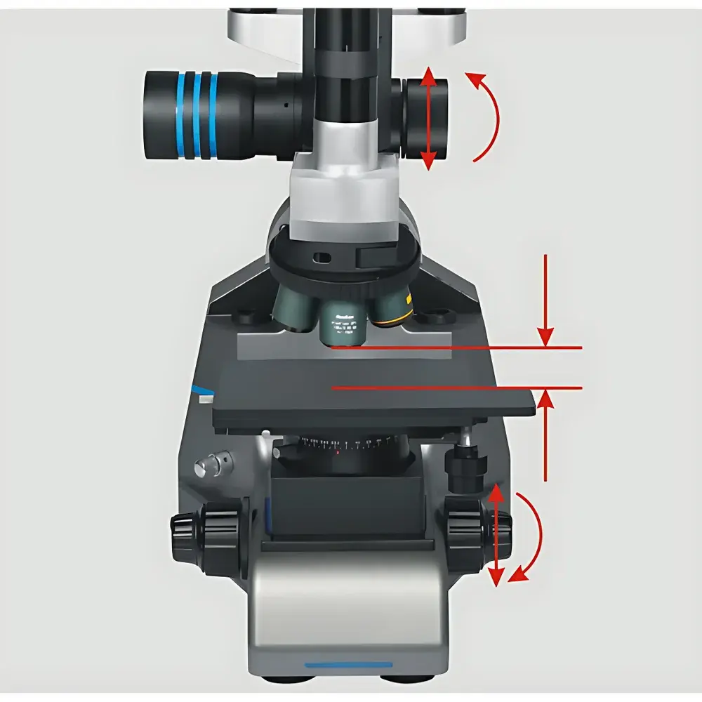
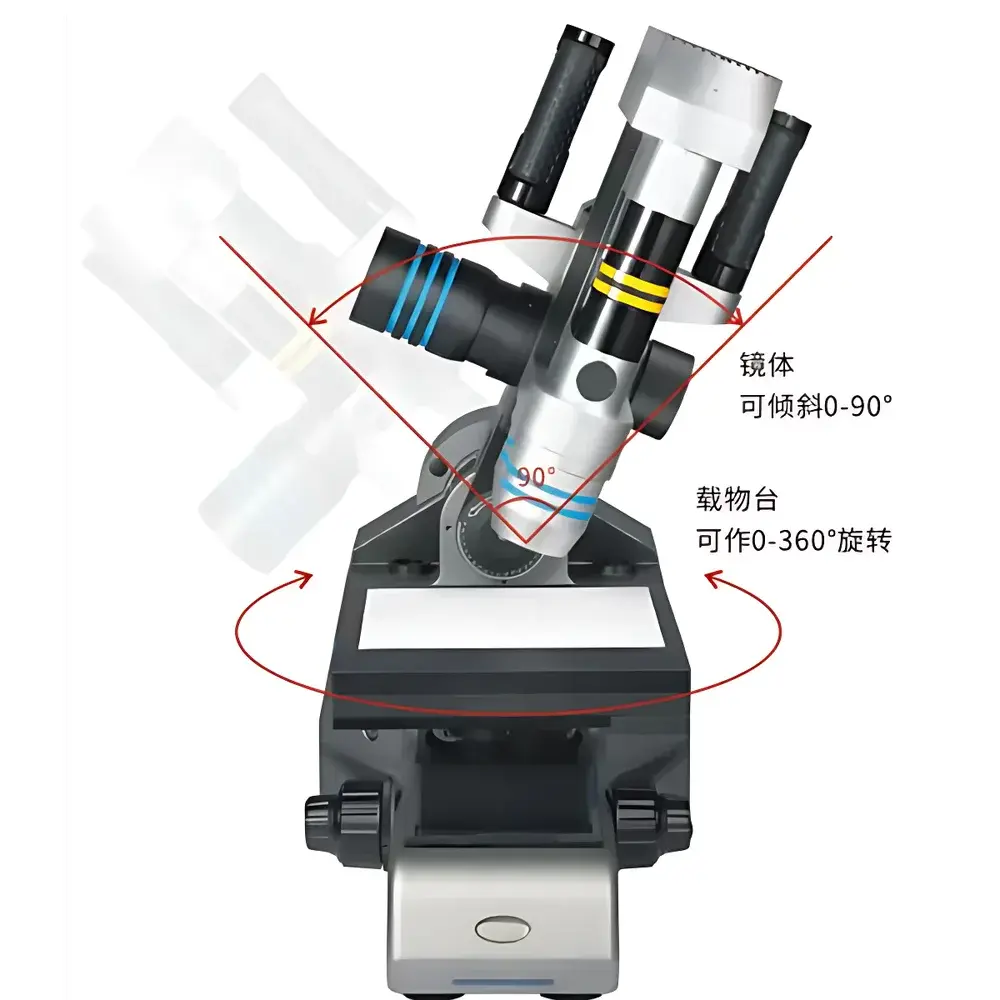
| Tiltable Objective Arm | 0°–90° left/right inclination with electronic brake |
| Rotatable Stage | 360° continuous electric rotation |
| Software Functions | Real-time extended depth-of-field (EDF) fusion, auto-focus, 2D/3D stitching, 2D metrology, 3D topography reconstruction, roughness analysis, cleanliness assessment (optional), IMC thickness measurement (optional) |
| Lens Type | Apochromatic corrected optics |
| Illumination Modes | Ring, diffuse, oblique, coaxial epi-illumination, transmitted, hybrid, brightfield, darkfield, polarized, DIC |
Overview
The LEI-TECH LK-CJS6300 Ultra-Deep Depth of Field Digital Microscope System is an engineered solution for high-fidelity surface inspection and quantitative 3D morphological analysis in industrial R&D, quality control, and failure analysis laboratories. Unlike conventional optical microscopes constrained by shallow depth of field at high magnifications, the LK-CJS6300 employs a hybrid optical-digital architecture: apochromatically corrected optics deliver diffraction-limited resolution and chromatic fidelity across the visible spectrum, while synchronized motorized Z-axis stepping—combined with real-time image fusion algorithms—enables pixel-accurate depth stacking without mechanical drift or focus breathing. This methodology conforms to the principles of extended depth-of-field (EDF) imaging as defined in ISO 25178-601 for areal surface texture characterization. The system operates as a non-contact, label-free metrology platform capable of generating calibrated 3D topographic maps with sub-micron vertical repeatability—essential for semiconductor wafer inspection, precision machining validation, and microelectronics intermetallic compound (IMC) layer thickness assessment.
Key Features
- Apochromatic optical train eliminating secondary spectrum and axial chromatic aberration—ensuring faithful color reproduction and minimal geometric distortion across the full magnification range
- Dual-configurable magnification paths: standard 30×–500× or ultra-high-resolution 80×–6500× objective turret, both compatible with EDF acquisition and 3D reconstruction workflows
- Motorized XYZ stage with 1 µm X/Y positional resolution and 0.1 µm Z-axis step resolution over 30 mm travel—fully programmable via software API for repeatable multi-point inspection routines
- Electronically actuated tilting arm (0°–90°) with tactile thumb-button brake—enabling rapid repositioning and stable angled observation without manual locking mechanisms
- 360° continuously rotating motorized stage with zero-backlash gearing—supporting comprehensive circumferential inspection of cylindrical or asymmetric components
- Multi-mode illumination engine supporting brightfield, darkfield, polarized, differential interference contrast (DIC), coaxial epi-illumination, transmitted light, and hybrid illumination protocols—all software-selectable and intensity-tunable
- Ruggedized aluminum alloy chassis with vibration-damping composite interface pads—optimized for stability during high-magnification EDF acquisition and large-area stitching
Sample Compatibility & Compliance
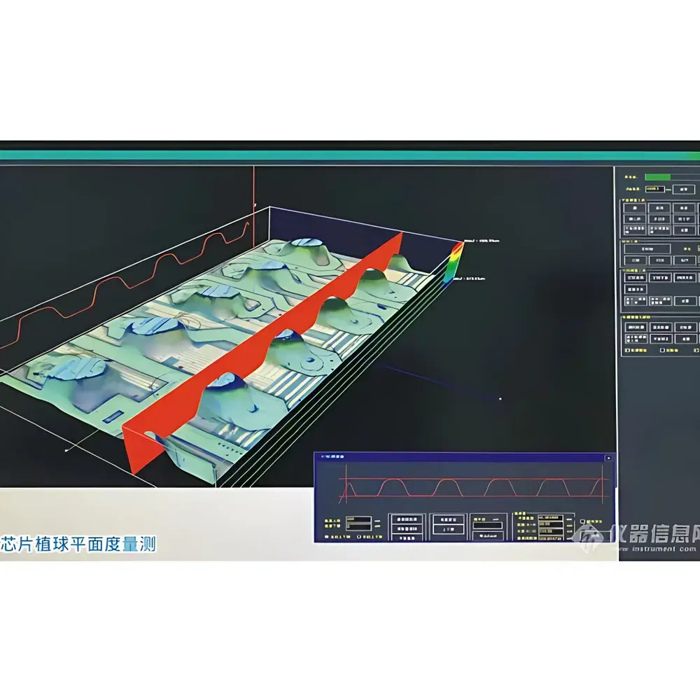
The LK-CJS6300 accommodates samples up to 205 mm × 180 mm × 120 mm (W × D × H) on its motorized stage, with optional extended-height configurations available. Its modular design supports integration into cleanroom environments (ISO Class 5–7) and manufacturing cells compliant with IATF 16949 and IPC-A-610 standards. The system’s measurement traceability aligns with ISO/IEC 17025 requirements when used with NIST-traceable calibration artifacts. All software-driven measurements—including height, angle, radius, roughness (Sa, Sq, Sz per ISO 25178-2), and cleanliness classification (per ISO 4406 and VDA 19.1)—generate audit-ready reports with embedded metadata, timestamps, operator ID, and instrument calibration status—meeting GLP/GMP documentation expectations and FDA 21 CFR Part 11 electronic record integrity criteria.
Software & Data Management
The proprietary LEI-Vision™ acquisition and analysis suite provides a unified interface for hardware control, image processing, and metrological reporting. Core capabilities include real-time EDF fusion at full 4K resolution (3840 × 2160 @ 60 fps), automated Z-stack acquisition with user-defined step intervals, and GPU-accelerated 3D point-cloud generation. Measurement modules support ISO-compliant 2D feature analysis (line, circle, distance, angle, radius) and 3D surface metrics (roughness, waviness, slope, volume). Optional add-ons enable IMC layer quantification (intermetallic thickness mapping via grayscale thresholding and cross-sectional profiling), pore analysis (ISO 4527), and particle-based cleanliness grading (VDA 19.2). All data exports are structured in CSV, TIFF (with embedded scale metadata), and STL formats—compatible with third-party CAE platforms such as ANSYS SpaceClaim and Metrolog X4. Audit trails record every parameter change, image save, and report export, satisfying regulatory requirements for data integrity and version control.
Applications
- Semiconductor & PCB: SMT solder joint inspection, wire bond morphology, die surface defect mapping, micro-cut cross-section topography, and underfill void analysis
- Precision Engineering: Thread pitch verification, gear tooth profile deviation, micro-machined surface finish evaluation (Ra, Rz), and burr detection on medical implants
- Materials Science: Grain boundary visualization in sintered ceramics, phase distribution in multiphase alloys, and oxidation layer thickness quantification on thermal barrier coatings
- Forensic & Document Examination: Ink differentiation, paper fiber structure analysis, latent impression recovery, and security feature validation (holograms, microprinting)
- Life Sciences (non-invasive): Histological slide screening, pollen morphology, insect cuticle microstructure, and biomaterial scaffold porosity assessment
FAQ
Does the LK-CJS6300 support automated batch inspection workflows?
Yes—the system integrates with LEI-Vision™ scripting engine and supports custom macro sequences for unattended multi-location imaging, EDF stacking, and measurement reporting. It also offers OPC UA and Modbus TCP interfaces for MES/SCADA connectivity.
Is calibration certification included with delivery?
Each unit ships with a factory calibration certificate covering optical magnification accuracy, stage positioning linearity, and Z-axis step repeatability—traceable to national metrology institutes. On-site recalibration services are available globally.
Can the system perform roughness analysis per ISO 25178 standards?
Yes—when equipped with the 3D Topography module, it calculates Sa, Sq, Sz, Sk, Spk, and other areal parameters directly from fused Z-stacks, with filter settings compliant with Gaussian robust filtering (ISO 16610-61).
What file formats are supported for data export and long-term archiving?
Raw images (12-bit TIFF with embedded scale bar and Z-step metadata), processed 3D point clouds (PLY, OBJ), measurement reports (PDF/XLSX with digital signature), and project files (LEI-Vision native format with full parameter history).
Is remote technical support available outside business hours?
LEI-TECH provides 7×24 remote diagnostics and screen-sharing assistance via secure TLS-encrypted channels, backed by regional service centers across North America, EMEA, and APAC.


