LPKF ProtoLaser Series Laser Micromachining Systems for Flexible Electronics Fabrication
| Brand | LPKF |
|---|---|
| Origin | Germany |
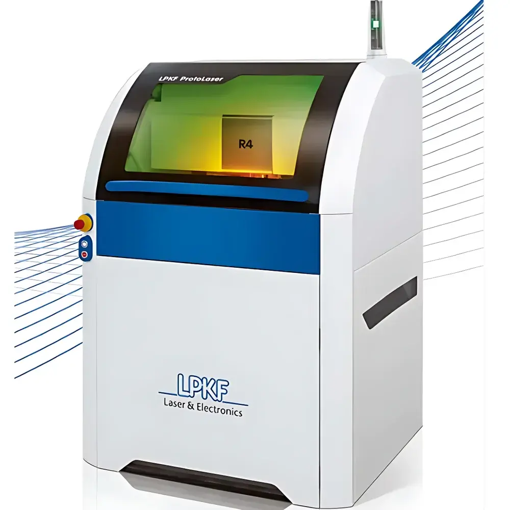
| Model | LPKF ProtoLaser H4 / S4 / U4 / R4 |
| Laser Types | Nanosecond Green (532 nm), Nanosecond UV (355 nm), Picosecond Green (515 nm), Mechanical + Laser Hybrid |
| Max. Processing Accuracy | 100 µm line width / 50 µm spacing |
| Safety Class | Class 1 Laser System |
| Footprint | < 1 m² |
| Power Supply | Standard AC Outlet + Compressed Air (6 bar) |
Overview
The LPKF ProtoLaser Series comprises four purpose-engineered laser micromachining platforms designed for rapid, high-precision prototyping and small-batch fabrication of electronic circuits—particularly on rigid, flexible, ceramic, and thermally sensitive substrates. Unlike conventional subtractive PCB milling or additive printing methods, the ProtoLaser systems employ controlled pulsed laser ablation to selectively remove conductive and dielectric layers with minimal thermal impact. Each variant leverages a distinct laser source optimized for specific material interaction physics: nanosecond green (532 nm) for copper-clad FR4 and RF laminates; nanosecond ultraviolet (355 nm) for cold ablation of polyimide, PTFE, LTCC, ITO/TCO, and ceramic substrates; picosecond (515 nm) for ultra-low-heat-load processing of ultra-thin flex foils, glass, sapphire, and brittle dielectrics; and hybrid mechanical–laser (H4) for simultaneous drilling, routing, and fine-feature laser patterning on thick multilayer boards. All systems operate under Class 1 laser safety certification—fully enclosed, interlocked, and compliant with IEC 60825-1—eliminating the need for external laser enclosures or operator PPE during routine operation.
Key Features
- Integrated vacuum chuck with programmable suction zones ensures flat, distortion-free substrate holding across diverse materials—from 25 µm polyimide films to 3 mm FR4 panels.
- High-resolution CCD vision system with automatic fiducial recognition enables sub-pixel alignment accuracy (< ±2 µm) for multi-layer registration and double-sided processing.
- CircuitPro CAM software provides guided workflow from Gerber import to toolpath optimization, including automatic laser parameter selection based on material stack-up, layer thickness, and feature geometry.
- Modular laser head design allows field-swappable optics and beam delivery modules without recalibration—supporting future upgrades and maintenance efficiency.
- All units are self-contained: powered by standard 230 V AC supply and require only clean, oil-free compressed air (6 bar) for vacuum generation and assist gas (optional N₂ purge for oxidation-sensitive metals).
- Compact footprint (< 0.95 m²) and integrated industrial PC enable deployment in ISO Class 7 cleanrooms, university labs, or R&D pilot lines without dedicated infrastructure.
Sample Compatibility & Compliance
The ProtoLaser platform supports a broad spectrum of electronic substrates validated per industry-standard material specifications: copper-clad polyimide (Kapton®), PET, PEN, PTFE (Rogers RO4000®), LTCC (DuPont 951), HTCC, FR4, alumina, quartz, silicon wafers, and transparent conductive oxides (ITO, FTO, AZO). Processing parameters adhere to IPC-2221B design guidelines for trace width tolerance and edge roughness (Ra < 1.2 µm typical). The systems meet CE marking requirements under Machinery Directive 2006/42/EC and EMC Directive 2014/30/EU. For regulated environments—including medical device prototyping and aerospace electronics development—the CircuitPro Advanced Edition supports audit-ready data logging compliant with FDA 21 CFR Part 11 (electronic signatures, change history, user access control) and GLP/GMP documentation workflows.
Software & Data Management
CircuitPro CAM is a Windows-based, offline-capable engineering suite delivering deterministic process repeatability. The Basic Edition (H4) handles single- and multi-layer rigid PCBs with automated drill-to-copper registration and contour compensation. The Advanced Edition (S4/U4/R4) extends functionality to flexible circuit definition—including dynamic bend zone modeling, strain-aware routing, and ceramic via filling simulation. All versions generate native G-code with embedded laser pulse energy modulation, spot overlap control, and Z-height compensation for warped substrates. Raw process logs—including laser power stability traces, vacuum pressure curves, and camera alignment residuals—are timestamped and exportable as CSV or SQLite databases for traceability and statistical process control (SPC) integration.
Applications
- Rapid iteration of RF/microwave antennas, filters, and impedance-matched transmission lines on low-Dk laminates.
- Prototyping of stretchable electrodes, biosensor interconnects, and microfluidic electrode arrays on elastomeric substrates.
- Low-volume fabrication of hybrid ceramic packages, MEMS interposers, and high-frequency sensor substrates.
- Repair and rework of defective traces or vias on populated boards without thermal damage to adjacent components.
- Research-grade fabrication of graphene, MXene, and printed perovskite device architectures requiring sub-50 µm feature fidelity.
- Education and training in advanced packaging, flexible hybrid electronics (FHE), and microfabrication process development.
FAQ
What laser safety classification applies to the ProtoLaser systems?
All ProtoLaser models are certified Class 1 laser products per IEC 60825-1:2014. The fully interlocked enclosure eliminates exposure risk during normal operation—no additional laser safety officer (LSO) oversight or facility modifications required.
Can CircuitPro software import industry-standard Gerber and ODB++ files?
Yes. CircuitPro natively imports Gerber RS-274X (with Aperture Macros), IPC-2581, and ODB++ formats. Layer stack-up definitions, netlist association, and solder mask expansion rules are preserved during translation.
Is nitrogen assist gas mandatory for processing copper layers?
Not mandatory—but recommended for high-speed, high-fidelity copper ablation on polyimide. N₂ purging suppresses oxide formation and improves edge quality; compressed air may be used for cost-sensitive academic applications where slight discoloration is acceptable.
How is calibration maintained across different substrate thicknesses?
The integrated CCD autofocus system dynamically adjusts focal plane position using real-time contrast analysis of surface features—no manual Z-height calibration is needed between runs, even when switching from 12 µm foil to 2.4 mm ceramic.
Does LPKF provide application-specific process recipes?
Yes. LPKF supplies validated parameter libraries for >60 common material combinations—including Rogers RO3003™, DuPont Pyralux® AP, Heraeus Cerasolzer® LTCC, and Toray Pyrolytic Graphite—available through secure customer portal access and updated quarterly.


