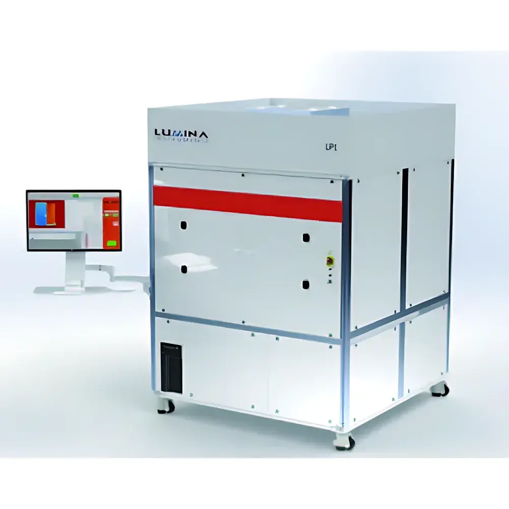
Lumina AT Series Optical Surface Defect Analyzer
| Brand | Lumina |
|---|---|
| Origin | USA |
| Manufacturer Type | Authorized Distributor |
| Origin Category | Imported |
| Model | AT Series (AT1, AT1-Auto, AT2, AT2-EFEM) |
| Pricing | Available Upon Request |
Overview
The Lumina AT Series Optical Surface Defect Analyzer is a high-precision, non-contact laser scanning inspection system engineered for semiconductor wafer and advanced optical material characterization. Based on multi-angle laser scattering combined with ellipsometric reflectance, surface slope mapping, and differential interference contrast principles, the AT Series detects sub-surface and surface anomalies—including particles, scratches, pits, bumps, residues, stress-induced birefringence, and thin-film thickness non-uniformities—without physical contact or sample preparation. Designed specifically for R&D labs and high-mix production environments in compound semiconductor, power device, and AR/VR optics manufacturing, it delivers quantitative defect metrology across both transparent and opaque substrates, including SiC, GaN, sapphire, fused silica, lithium niobate, InP, and silicon wafers up to 300 mm × 300 mm.
Key Features
- Multi-Channel Detection Architecture: Four synchronized optical channels operate simultaneously—each optimized for distinct scattering regimes (e.g., forward scatter, backscatter, polarization-resolved reflectance)—enabling concurrent classification of particle type, location (top surface, buried interface, or substrate), and morphology.
- Sub-Nanometer Sensitivity: Capable of resolving surface contaminants as small as 0.5 nm RMS height variation on ultra-smooth films; achieves 70 nm PSL (Polystyrene Latex) sensitivity on silicon and 150 nm PSL on glass substrates under standard operating conditions.
- Universal Sample Handling: Patented dual-pin vacuum chuck system accommodates irregular shapes, ultra-thin (<100 µm) or fragile substrates (e.g., SOI, GaN-on-sapphire), and variable thicknesses (0.1–5 mm) without mechanical clamping stress.
- High-Throughput Scanning: Full-field inspection of a 150 mm wafer completed in ≤180 seconds at standard resolution; AT2 variants support up to 300 mm × 300 mm planar samples with automated stage positioning and stitching algorithms.
- Non-Destructive Multi-Layer Discrimination: By dynamically adjusting incident laser angle and analyzing phase-shifted reflectance signatures, the system distinguishes between top-surface contamination, interfacial delamination, and bulk subsurface defects—critical for TSV, epitaxial layer, and bonding interface evaluation.
Sample Compatibility & Compliance
The AT Series supports broad material compatibility: transparent dielectrics (quartz, sapphire, BK7, CaF₂), semiconductors (Si, SiC, GaN, InP, GaAs), piezoelectric crystals (LiNbO₃), and metallized substrates (TiN, Al, Cu). All models comply with ISO 14644-1 Class 5 cleanroom operational requirements and integrate seamlessly into existing fab infrastructure via SECS/GEM protocol support. Data acquisition meets FDA 21 CFR Part 11 and EU Annex 11 compliance standards when configured with audit-trail-enabled software packages—ensuring traceability for GLP/GMP-regulated development and qualification workflows.
Software & Data Management
Lumina’s proprietary DefectIQ™ analysis suite provides real-time defect classification using supervised machine learning trained on >12,000 labeled reference defects across 17 material classes. Classification outputs include defect type (particle, scratch, pit, residue, haze), spatial coordinates (X/Y/Z), size distribution histograms, and severity ranking based on scattering cross-section and optical contrast. All results export natively to CSV, XML, and industry-standard SEMI E142 format. Optional diamond-scribe module enables precise physical marking of critical defects for downstream SEM/FIB cross-sectioning. Software includes full version control, user-role-based access permissions, and integrated report generation compliant with internal quality management systems (QMS) and IATF 16949 documentation protocols.
Applications
- Compound Semiconductor Manufacturing: In-line monitoring of SiC and GaN epi-wafers for micropipe density, hillock formation, and carbon inclusion detection prior to device fabrication.
- AR/VR Waveguide Metrology: Quantitative assessment of grating fidelity—including edge roughness, sidewall angle deviation, and buried particulate contamination—on replicated polymer and glass waveguides.
- Optical Component Qualification: Residual stress mapping on precision lenses, Fresnel arrays, and photomask blanks via localized birefringence analysis.
- Advanced Packaging: Detection of voids, filler agglomerates, and interfacial delamination in fan-out wafer-level packaging (FOWLP) and chip-to-wafer bonding stacks.
- MEMS & Photonics Fabrication: Identification of stiction-related surface deformation, release etch residues, and coating non-uniformity on suspended membranes and micro-lens arrays.
FAQ
What defect types can the AT Series detect on transparent substrates?
It identifies surface particles, embedded bubbles, subsurface cracks, polishing-induced scratches, residual organic/inorganic films, and localized stress-induced birefringence—without requiring index-matching fluids.
Can the system differentiate between top-surface and bottom-surface defects on a double-side-polished wafer?
Yes—by correlating angular-dependent scattering intensity profiles with ellipsometric phase data, it assigns Z-depth confidence intervals with ±0.8 µm resolution for defects within 10 µm of either interface.
Is EFEM integration supported for AT2-EFEM models?
Yes—AT2-EFEM includes SMIF/FOUP load ports, vacuum-compatible robotics interface, and full SECS/GEM v5.0 compliance for direct integration into 200 mm and 300 mm automated process lines.
Does the system require periodic recalibration?
No routine recalibration is needed; built-in NIST-traceable reference standards and automated daily self-check routines ensure long-term measurement stability per ISO/IEC 17025 guidelines.
What file formats are supported for defect map export?
CSV (coordinate + classification), SEMI E142 (defect summary), TIFF (high-res grayscale scan image), and JSON (structured metadata for MES integration).
Related Products


