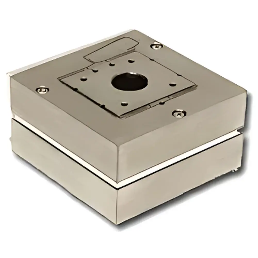

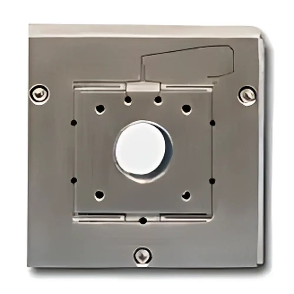
MCL Think Nano Nano-M250 Dual-Axis Piezoelectric Nanopositioning Stage
| Brand | MCL Think Nano |
|---|---|
| Origin | USA |
| Model | Nano-M250 |
| Motion Range (XY) | 50 μm × 50 μm |
| Aperture | 0.5 inch |
| Control | Closed-loop |
| Resolution | 0.1 nm |
| Resonant Frequency (X) | 1.0 kHz ±20% |
| Resonant Frequency (Y) | 700 Hz ±20% |
| Stiffness | 1.0 N/μm |
| Angular Deviation (Roll/Pitch) | ≤1 μrad |
| Angular Deviation (Yaw) | ≤3 μrad |
| Max Load (Horizontal) | 0.5 kg |
| Max Load (Vertical) | 0.2 kg |
| Body Material | Invar or Titanium |
| Vacuum Compatibility | Available for HV/UHV |
Overview
The MCL Think Nano Nano-M250 is a high-precision, dual-axis piezoelectric nanopositioning stage engineered for sub-nanometer motion control in demanding optical and scanning probe applications. Based on capacitive-sensed closed-loop operation and proprietary PicoQ® position feedback technology, the Nano-M250 delivers absolute, drift-free positional stability with 0.1 nm resolution and 50 μm × 50 μm bidirectional travel range. Its monolithic titanium or Invar construction ensures exceptional thermal stability and mechanical rigidity—critical for maintaining alignment integrity during extended acquisition cycles in scanning electron microscopy (SEM), atomic force microscopy (AFM), and laser interferometry setups. The integrated 0.5-inch central aperture enables unobstructed optical access or feedthrough routing for fiber optics, electrical probes, or vacuum-compatible manipulators—making it suitable for both ambient and high-vacuum (HV) or ultra-high-vacuum (UHV) environments when specified.
Key Features
- Monolithic design fabricated from low-expansion Invar or lightweight, non-magnetic titanium—optimized for thermal and mechanical stability
- True closed-loop control architecture with integrated capacitive position sensors delivering real-time, absolute position feedback
- PicoQ® sensing technology enabling picometer-level repeatability and long-term positional fidelity without recalibration
- Compact footprint (≤75 mm × 75 mm base) facilitating seamless integration into space-constrained instruments including SEM columns, confocal microscopes, and lithography tooling
- Resonant frequencies of 1.0 kHz (X-axis) and 700 Hz (Y-axis) supporting high-speed raster scanning with minimal phase lag and dynamic tracking error
- Stiffness of 1.0 N/μm ensures minimal hysteresis and load-induced deflection—even under active probing or optical trapping loads
- Angular deviations limited to ≤1 μrad (roll/pitch) and ≤3 μrad (yaw), preserving beam collimation and probe tip orientation across full travel
Sample Compatibility & Compliance
The Nano-M250 is designed for compatibility with standard optical breadboards (M4/M6 tapped holes), SEM stubs, and vacuum flanges (CF-35 or KF-40 configurable upon request). All HV/UHV variants undergo rigorous outgassing testing per ASTM E595 and are assembled using vacuum-rated adhesives and ceramics. The stage meets ISO 9001-certified manufacturing protocols and supports GLP/GMP-aligned workflows through traceable calibration documentation. When operated with the Nano-Drive® controller, system behavior complies with FDA 21 CFR Part 11 requirements for electronic records and signatures—enabling audit-ready data logging in regulated R&D and QC environments.
Software & Data Management
Control is enabled via the Nano-Drive® digital controller, which provides USB 2.0 and Ethernet interfaces alongside analog I/O for synchronization with external triggers (e.g., laser pulses, detector gates). The accompanying Nano-Control™ software suite supports scripting (Python API), real-time waveform generation (sine, sawtooth, Lissajous), and synchronized multi-axis acquisition. All position data are timestamped with microsecond precision and stored in HDF5 format—ensuring interoperability with MATLAB, Python (NumPy/Pandas), and LabVIEW-based analysis pipelines. Audit trails—including parameter changes, calibration events, and user logins—are retained with SHA-256 hashing for regulatory compliance.
Applications
- Active alignment of single-mode fibers and photonic integrated circuits (PICs) in free-space and fiber-coupled optical systems
- Nanolithography stage for electron-beam and focused ion-beam (FIB) direct-write systems requiring sub-10 nm overlay accuracy
- Scanning probe microscopy (SPM) XY scanner for AFM, STM, and near-field optical microscopy (SNOM)
- Beam steering and focus correction in adaptive optics testbeds and ultrafast laser pulse compression setups
- In-situ nanomechanical testing stages compatible with TEM/SEM sample holders and nanoindenter integration
- Quantum device characterization platforms requiring cryogenic-compatible positioning (optional low-temp variants available)
FAQ
What vacuum levels is the Nano-M250 rated for?
Standard models operate in ambient air; HV-compatible versions are qualified to 1×10⁻⁷ Torr, and UHV variants meet 1×10⁻¹¹ Torr specifications with all-metal seals and bake-out capability.
Can the Nano-M250 be used in cryogenic environments?
Yes—custom configurations with low-thermal-contract materials and cold-stage mounting interfaces are available for operation down to 4 K; consult engineering for thermal contraction compensation profiles.
Is third-party software integration supported?
Full API support is provided for Python, MATLAB, LabVIEW, and C/C++; DLLs and header files are included with the Nano-Drive® SDK.
How is calibration traceability maintained?
Each unit ships with NIST-traceable calibration certificates covering linearity, orthogonality, and sensor gain—valid for 12 months under normal operating conditions.
What maintenance is required for long-term performance?
No routine maintenance is required; the solid-state piezoelectric actuation and frictionless flexure guidance eliminate wear mechanisms—only periodic verification against reference interferometers is recommended for metrology-grade applications.


