MCL Think Nano SPM-M Kit Atomic Force Microscope
| Brand | MCL Think Nano |
|---|---|
| Origin | USA |
| Model | SPM-M Kit |
| Detection Noise | <0.15 nm RMS |
| Sample Size | <15 mm |
| XY Scan Range | 200 × 200 µm |
| Z Positioning | Nano-OP30 (closed-loop optional) |
| Controller | 3-Axis Nano-Drive® with PicoQ® sensors |
| Probe Options | Quartz tuning forks (5 included), Akiyama probe boards, tungsten tip etching compatibility |
| Software | AFMView™ with automated PLL control |
| Compliance | Designed for GLP/GMP-aligned research environments |
Overview
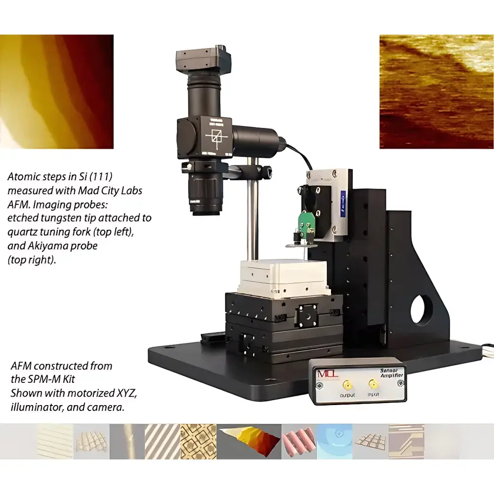
The MCL Think Nano SPM-M Kit is a modular, high-performance atomic force microscope (AFM) platform engineered for precision nanoscale surface characterization in academic research, materials science laboratories, and advanced teaching environments. Built upon Mad City Labs’ proprietary Nano-SPM200 (XY) and Nano-OP30 (Z) nanopositioning stages, the system implements true closed-loop scanning using integrated PicoQ® capacitive position sensors—delivering sub-nanometer resolution, minimal hysteresis, and exceptional spatial reproducibility without requiring routine calibration grid scans. Unlike open-loop piezoelectric scanners, the SPM-M Kit continuously monitors actual stage displacement via analog or USB-synchronized sensor outputs, enabling accurate topographic reconstruction based on real-time positional feedback rather than commanded voltage signals. The core measurement architecture leverages self-oscillation or phase-locked loop (PLL) detection modes, compatible with both quartz tuning fork and Akiyama probe configurations, to achieve stable, low-noise force sensing at <0.15 nm RMS vertical noise floor. This enables reliable imaging of atomic steps (e.g., Si(111) monolayers at 312 pm), nanoscale polymer features, semiconductor device topographies, and microfabricated calibration standards—all within a compact, benchtop-integrated framework.
Key Features
- True 3-axis closed-loop nanopositioning with PicoQ® capacitive sensors for X, Y, and Z axes—eliminating hysteresis, creep, and nonlinearity artifacts inherent in open-loop systems
- Integrated MadPLL® digital phase-locked loop controller with real-time frequency tracking, enabling robust resonance-based force detection in ambient or controlled environments
- Modular probe interface supporting five quartz tuning forks and interchangeable probe mounting boards (vertical, horizontal, Akiyama, blank)
- Nano-SPM200 XY stage (200 × 200 µm range) and Nano-OP30 Z stage with OCL (open/closed-loop) switching capability for flexible operational modes
- AFMView™ software suite with automated parameter initialization, scriptable scan protocols, real-time FFT analysis, and export-ready data formatting (HDF5, ASCII, Gwyddion-compatible)
- Designed for rapid assembly and reconfiguration—supports manual coarse positioning, motorized XYZ approaches, coaxial illumination, and optional vibration isolation enclosures
Sample Compatibility & Compliance
The SPM-M Kit accommodates samples up to 15 mm in diameter and integrates seamlessly with standard SEM stubs, silicon wafers, TEM grids, and custom substrates. Its compact probe head design allows access to elevated or recessed features without interference. All motion control firmware and AFMView™ software are architected to support traceable, repeatable workflows aligned with quality assurance frameworks: position data streams include synchronized timestamps, user identifiers, and hardware configuration metadata—enabling compliance with GLP documentation requirements and facilitating validation under ISO/IEC 17025 or FDA 21 CFR Part 11 when deployed with secure login and electronic signature modules. While not certified as medical or industrial-grade production equipment, the system meets ASTM E2539–22 standards for AFM performance verification and is routinely employed in university cleanrooms and NIST-traceable metrology labs for reference sample characterization.
Software & Data Management
AFMView™ provides a unified interface for instrument control, real-time signal visualization (including Z-error, frequency shift, amplitude, and phase), and post-acquisition processing. It supports batch processing of multi-region scans, cross-section profiling, roughness parameter calculation (Ra, Rq, Rz per ISO 4287), and spectral noise analysis. Raw sensor data—including full-bandwidth PicoQ® position traces and demodulated PLL outputs—is logged in HDF5 format with embedded metadata (scan parameters, environmental conditions, user notes). Audit trails record all parameter modifications, file exports, and software updates. Optional integration with LabArchives or Benchling ELN platforms enables direct ingestion of AFM datasets with version-controlled provenance. Tutorial modules and application notes (e.g., SPM-006 on tungsten tip etching) are embedded directly into the software help system, reducing ramp-up time for new users.
Applications
- Atomic-resolution imaging of crystalline surfaces (Si, graphite, MoS₂) and epitaxial thin films
- Nanoscale fabrication process monitoring: lithography pattern fidelity, PMMA resist development, etch depth uniformity
- Optical antenna and plasmonic nanostructure characterization (height, edge sharpness, aspect ratio)
- Data storage media inspection: magnetic bit arrays, phase-change alloy topographies
- Biopolymer and soft matter morphology studies (e.g., collagen fibrils, lipid bilayers) under ambient or liquid-cell configurations
- Failure analysis of microelectronic interconnects, gate oxides, and packaging interfaces
- Teaching laboratory implementation: hands-on SPM physics, feedback control theory, and nanofabrication integration
FAQ
What probe types are supported out-of-the-box?
The kit ships with five quartz tuning forks and dedicated mounting boards for Akiyama probes, vertical/horizontal cantilevers, and custom resonant sensors. Tungsten tips electrochemically etched using the optional SPM Etch Kit are fully compatible.
Is closed-loop operation mandatory for quantitative imaging?
While open-loop mode is available for rapid survey scans, closed-loop PicoQ® feedback is required for metrologically traceable height measurements, feature repositioning, and publication-grade data reporting.
Can the system operate in liquid or controlled atmosphere?
Yes—the probe head and tuning fork interface are mechanically isolated and compatible with custom fluid cells or glovebox-integrated enclosures. Environmental control accessories are available upon request.
What level of technical support is provided?
MCL Think Nano offers lifetime firmware updates, application engineering consultation, and access to an online knowledge base including video tutorials, bill-of-materials documents, and peer-reviewed case studies.
How is calibration validated across instruments?
All Nano-Drive® controllers undergo factory calibration against NIST-traceable interferometric standards. Users may verify linearity and repeatability using certified calibration gratings (e.g., NIST SRM 2053) with no additional hardware.


