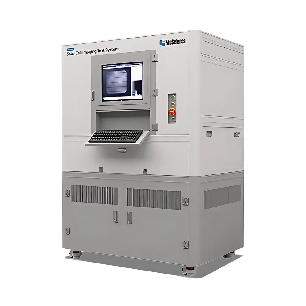
McScience K3300PLX Photoluminescence & Electroluminescence Defect Inspection System for Solar Cells
| Brand | McScience |
|---|---|
| Origin | Imported |
| Manufacturer Type | Authorized Distributor |
| Model | K3300PLX |
| Pricing | Available Upon Request |
Overview
The McScience K3300PLX is a high-resolution, multi-modal luminescence and optoelectronic imaging platform engineered for non-destructive defect characterization of silicon photovoltaic (PV) cells and modules. It operates on the physical principles of carrier injection and radiative recombination: electroluminescence (EL) imaging applies forward bias to induce minority-carrier injection and subsequent infrared photon emission; photoluminescence (PL) imaging uses calibrated broadband or monochromatic excitation (e.g., 850 nm or 940 nm LEDs or lasers) to generate excess carriers without electrical contact; light-beam-induced current (LBIC) mapping measures local photocurrent response under focused illumination; and thermal imaging captures Joule heating signatures associated with shunts, series resistance anomalies, or microcrack-induced current crowding. The system integrates synchronized stage motion, low-noise scientific CMOS imaging, and calibrated optical filtering to deliver quantitative, spatially resolved contrast maps correlated directly with device physics—enabling root-cause analysis of performance-limiting defects at wafer, cell, and module levels.
Key Features
- Multi-modal acquisition architecture supporting simultaneous or sequential EL, PL, LBIC, and thermographic imaging in a single instrument platform
- High-sensitivity, cooled scientific CMOS camera with quantum efficiency >70% in 900–1100 nm range and pixel resolution up to 5.5 MP (2560 × 2160), optimized for near-infrared (NIR) luminescence detection
- Programmable LED or laser excitation source with adjustable intensity, pulse width (1 µs–1 s), and spectral output (optional 785 nm, 850 nm, or 940 nm configurations)
- Motorized XYZ translation stage with sub-10 µm repeatability and programmable scan patterns (raster, spiral, ROI-based), compatible with standard 156 mm × 156 mm to 210 mm × 210 mm PV formats
- Integrated bias supply (0–30 V, 0–10 A DC/AC) with real-time current monitoring and compliance limiting for safe EL operation on fragile heterojunction (HJT), TOPCon, and PERC devices
- Modular optical path with interchangeable bandpass filters (e.g., 1050 ± 25 nm for Si EL, 1150 ± 40 nm for PL), neutral density wheels, and optional polarization optics for anisotropic defect analysis
Sample Compatibility & Compliance
The K3300PLX accommodates bare wafers, textured or passivated cells (including bifacial and tandem architectures), mini-modules, and full-size commercial modules (up to 2.4 m × 1.3 m with extended stage option). Sample mounting is facilitated via vacuum chuck or kinematic fixture with thermal isolation. All imaging modes comply with established PV quality control protocols referenced in IEC 60904-13 (electroluminescence imaging), IEC 62788-7-2 (photoluminescence for crystalline silicon), and ASTM E2923-22 (non-contact inspection of PV materials). Data acquisition workflows support audit-ready metadata tagging—including operator ID, timestamp, environmental conditions (ambient temperature/humidity), and calibration certificate traceability—to align with GLP-compliant laboratory practices and internal quality management systems.
Software & Data Management
Control and analysis are executed through McScience’s proprietary K3300PLX Suite v4.x, a Windows-based application built on Qt and Python (NumPy, SciPy, OpenCV). The software provides real-time preview, multi-channel image registration, pixel-wise intensity normalization, defect segmentation using adaptive thresholding and morphological operators, and quantitative metrics including relative luminance uniformity (RLU), dark area fraction (DAF), and LBIC responsivity gradient. Export formats include TIFF (16-bit), HDF5 (for time-series or hyperspectral stacks), CSV (ROI statistics), and PDF reports compliant with ISO/IEC 17025 documentation requirements. Optional integration with LIMS via RESTful API enables automated data ingestion into enterprise QA databases. All user actions, parameter changes, and calibration events are logged with timestamps and digital signatures per FDA 21 CFR Part 11 Annex 11 guidelines.
Applications
- Detection and classification of microcracks, finger interruptions, busbar discontinuities, and edge chipping in mass-produced PERC, TOPCon, and HJT cells
- Identification of recombination-active grain boundaries, dislocation clusters, and metal impurity precipitation in multicrystalline and upgraded metallurgical-grade silicon
- Quantification of passivation layer integrity (e.g., SiNx:H, AlOx) via PL lifetime correlation and spatial decay mapping
- Root-cause analysis of hot spots in field-deployed modules using comparative EL/thermal overlays
- Process development feedback for screen printing, laser ablation, and firing furnace optimization through statistical process control (SPC) of defect density trends
- Pre-shipment inspection for Tier-1 manufacturers requiring traceable, repeatable, and standardized imaging results per customer technical agreements
FAQ
What types of solar cell technologies are supported by the K3300PLX?
The system is validated for monocrystalline and multicrystalline silicon (c-Si), thin-film CIGS and CdTe, and emerging technologies including perovskite-silicon tandems—provided the luminescence emission falls within the NIR detection range (800–1200 nm).
Can the K3300PLX be integrated into an inline production environment?
Yes—via optional conveyor interface, Ethernet/IP communication, and PLC-triggered acquisition sequences; however, full integration requires site-specific validation for vibration isolation, ambient light suppression, and thermal stability.
Is calibration traceable to national standards?
Radiometric calibration is performed using NIST-traceable silicon photodiode reference detectors and calibrated integrating sphere sources; spectral response is verified annually by an ISO/IEC 17025-accredited metrology lab.
Does the system support automated defect classification using AI?
The base software includes rule-based segmentation; optional AI modules (TensorFlow-based CNN models) trained on annotated industrial datasets can be licensed separately for supervised classification of crack morphology, shunt severity, and solder bond failure modes.
What maintenance is required for long-term operational stability?
Annual optical alignment verification, camera dark-frame update, LED/laser source intensity recalibration, and stage positional accuracy validation using interferometric reference standards are recommended per McScience’s Maintenance Protocol MP-K3300-02.


