MicroChem AZ1500 Series i-Line Positive Photoresist
| Brand | MicroChem Corp |
|---|---|
| Origin | Guangdong, China |
| Manufacturer Type | Authorized Distributor |
| Product Line | AZ1500 Series |
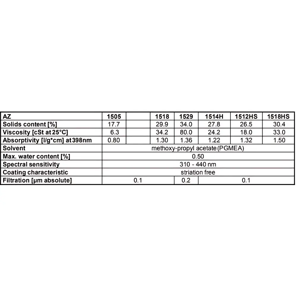
| Solvent System | Propylene Glycol Monomethyl Ether Acetate (PGMEA) |
| UV Sensitivity Range | 310–440 nm (i-, h-, g-line) |
| Recommended Development Time | AZ1500/AZ1514H: 50–60 s |
| AZ1500HS | 20–30 s |
| Compatible Developers | AZ 351B (1:4 dilution), 0.5% NaOH, AZ 726MIF |
| Film Thickness Range | 0.5–4.0 μm (spin-coated) |
| Storage Conditions | 0–25°C, sealed container, light-protected |
| Shelf Life | Batch-specific (see label: YYYY/MM/DD) |
| Compliance | Fully compatible with standard semiconductor cleanroom protocols and ISO Class 5–7 environments |
Overview
The MicroChem AZ1500 Series is a family of high-performance, PGMEA-based positive photoresists engineered for i-line (365 nm) photolithography in semiconductor fabrication, MEMS processing, and microelectronics R&D. Unlike legacy cellosolve acetate–based resists, the AZ1500 Series utilizes a proprietary, lower-toxicity solvent system while maintaining full spectral response across the mercury lamp’s primary UV emission lines—g-line (436 nm), h-line (405 nm), and i-line (365 nm). This broad-band sensitivity enables compatibility with both broadband and monochromatic exposure tools, including contact, proximity, and projection aligners. The series comprises three chemically differentiated variants—AZ1500 (standard), AZ1514H (high-exposure latitude), and AZ1500HS (high-speed, enhanced adhesion)—each formulated with tailored novolak resin molecular weight distributions to meet specific process requirements in wet etch, dry etch, and high-yield production environments.
Key Features
- PGMEA-based formulation: Replaces hazardous ethylene glycol ether acetates (e.g., CELLOSOLVE® AC) in alignment with ICH Q3C and OSHA-recommended solvent safety guidelines.
- Controlled photospeed tuning: AZ1500 exhibits ~5–10% higher photosensitivity than its AZ1370/AZ1450J predecessors due to reduced solvent volatility; compensated via minor prebake temperature adjustment (+5°C).
- Resolution capability: Consistently achieves ≥1 µm line/space resolution under standard i-line exposure and aqueous development—validated across 150 mm and 200 mm wafer platforms.
- Adhesion optimization: AZ1500HS employs low-MW novolak fractions to suppress “mousebite” defects at Al/SiO₂ interfaces during wet etching—a critical reliability factor in discrete device and bipolar IC manufacturing.
- Developer flexibility: Fully compatible with industry-standard alkaline developers—including AZ 351B (1:4), dilute NaOH (0.5 wt%), and metal-ion-free formulations such as AZ 726MIF—supporting both batch and spray development tools.
Sample Compatibility & Compliance
The AZ1500 Series demonstrates robust adhesion and process stability on silicon, silicon dioxide, silicon nitride, aluminum, titanium, and chromium substrates. It has been qualified for use in Class 100 (ISO 5) and Class 1,000 (ISO 6) cleanrooms and conforms to SEMI C1–C29 material purity specifications for trace metals (<1 ppb for Na, K, Fe, Cu, Ni, Cr). While not inherently compliant with FDA 21 CFR Part 11 or EU Annex 11 (as it is a consumable, not software-controlled instrumentation), its lot traceability, expiration coding (YYYY/MM/DD), and batch-specific Certificate of Analysis support full GLP/GMP documentation workflows. All resists are supplied in nitrogen-purged, amber HDPE or fluoropolymer-lined bottles to prevent photochemical degradation and moisture ingress.
Software & Data Management
As a photoresist material—not an instrument—the AZ1500 Series does not incorporate embedded firmware or data logging. However, its performance parameters (photospeed, contrast gamma, post-apply bake (PAB) window, development rate uniformity) are fully integrable into factory-wide process control systems (e.g., Applied Materials Endura®, Lam Research ALTUS®, or generic SPC platforms) via standardized recipe templates. MicroChem provides digital Certificates of Analysis (CoA) and Safety Data Sheets (SDS) in English, compliant with GHS Rev. 7 and REACH Annex II. Batch-level metrology data—including viscosity (measured per ASTM D1200), solids content (ASTM D2196), and spectral absorbance (per JIS K 5600-5-2)—are archived for ≥10 years and accessible upon request for audit readiness.
Applications
- Semiconductor front-end-of-line (FEOL) patterning for CMOS, BiCMOS, and power devices using i-line steppers and mask aligners.
- MEMS fabrication requiring high aspect ratio resist profiles and etch selectivity against SiO₂ and SiNₓ.
- Hybrid packaging and substrate lithography for fan-out wafer-level packaging (FOWLP) and interposer patterning.
- R&D prototyping in university cleanrooms and government labs where solvent safety, reproducibility, and rapid process transfer are prioritized over deep-UV capabilities.
- Legacy IC re-manufacturing where compatibility with existing AZ1350-series infrastructure (coaters, developers, etchers) is mandatory.
FAQ
What exposure wavelength range is supported by the AZ1500 Series?
The AZ1500 Series responds uniformly from 310 nm to 440 nm, covering the full i-line (365 nm), h-line (405 nm), and g-line (436 nm) mercury spectrum—enabling use with both broadband and filtered i-line sources.
Can AZ1500 be substituted directly for AZ1350J without process requalification?
Yes—AZ1500 is explicitly designed as a drop-in replacement for AZ1350J, AZ1450J, and AZ1370 in most i-line processes; however, a ±5°C adjustment to prebake temperature and verification of development time uniformity are recommended per SEMI E157-0317.
Is AZ1500HS suitable for plasma etch applications?
AZ1500HS is optimized for wet-etch processes (e.g., buffered oxide etch, Al etch); for dry etch (RIE, ICP), AZ1500 or AZ1514H is preferred due to higher etch resistance and carbon content.
How should expired AZ1500 resist be handled?
Do not use beyond the printed expiration date (YYYY/MM/DD). Expired resist may exhibit increased standing wave effects, reduced contrast, or inconsistent develop rates—potentially compromising CD control and defect density.
Are there restrictions on substrate priming when using AZ1500?
HMDS vapor priming is strongly recommended for Si/SiO₂ wafers; for Al or Ti substrates, oxygen plasma pretreatment improves adhesion—particularly critical for AZ1500HS to eliminate lift-off during long etch cycles.


