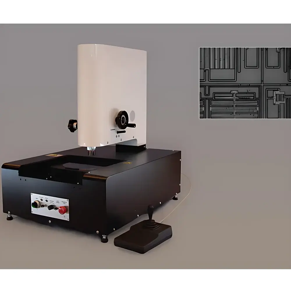
Midas IR-M Infrared Wafer Inspection Microscope
| Brand | Midas |
|---|---|
| Origin | Switzerland |
| Model | IR-M (Infrared Microscope) |
| Optical Magnification Options | 2.5×, 5×, 10× |
| Wafer Compatibility | 100 mm (4″), 150 mm (6″), 200 mm (8″) |
| Spatial Resolution | ≤3 µm (at 5× objective, transmission mode) |
| Detection Sensitivity | Defects ≥3 µm resolvable in Si wafers under IR transmission |
| Illumination Modes | Top-side visible illumination (reflected mode) + Through-wafer infrared illumination (transmission mode) |
| Imaging Sensor | IR-sensitive CMOS camera with USB 3.0 interface |
| Stage | Manual or motorized XY stage (Ø ≤200 mm wafer support) |
| Application Domain | Silicon IC & MEMS wafer-level defect inspection, SOI layer visualization, buried structure analysis |
Overview
The Midas IR-M Infrared Wafer Inspection Microscope is an engineered optical metrology platform designed specifically for non-destructive, high-contrast imaging of silicon-based semiconductor and MEMS wafers. Unlike conventional visible-light microscopes, the IR-M leverages near-infrared (NIR) transmission—typically at wavelengths between 900 nm and 1700 nm—to penetrate bulk silicon substrates that are opaque to visible light. This capability enables direct visualization of subsurface features including buried oxide (BOX) layers in SOI wafers, trench isolation structures, through-silicon vias (TSVs), MEMS device cavities, and interfacial delaminations. The system operates on the principle of differential IR absorption and scattering contrast, where variations in dopant concentration, crystal defects, or layer thickness modulate transmitted IR intensity. Its modular optical architecture integrates long-working-distance objectives, dual-path illumination (top-side visible + bottom-side IR), and a calibrated IR-sensitive imaging sensor—ensuring reproducible, traceable inspection across process development, inline QC, and failure analysis workflows.
Key Features
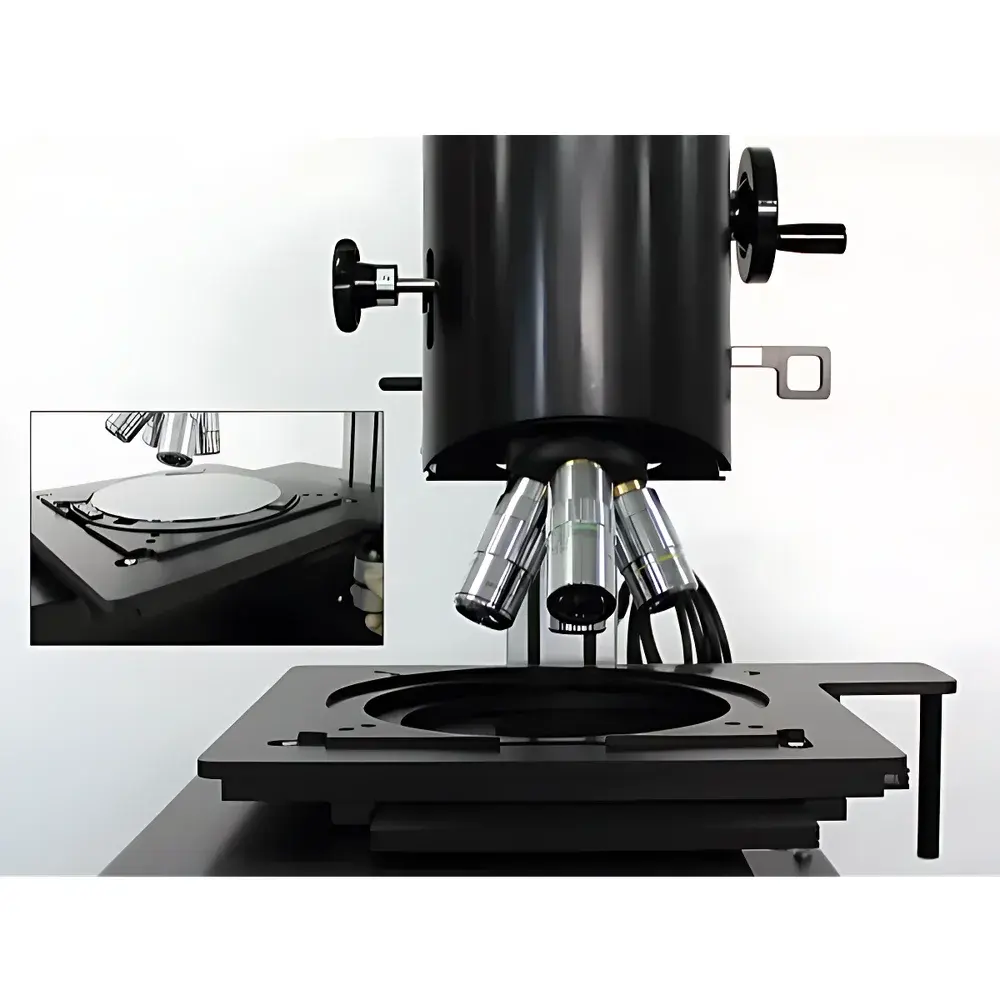
- Triple-magnification optical path (2.5×, 5×, 10×) with parfocal, long-working-distance IR-corrected objectives optimized for silicon transparency at 1310 nm and 1550 nm
- Sub-3 µm spatial resolution in transmission mode using the 5× objective—validated per ISO 10110-5 standards for optical component testing
- Dual illumination configuration: LED-based top-side white-light source for surface topology inspection (reflected mode), and collimated IR LED array (1310 nm nominal) for deep-substrate transmission imaging
- Motorized XY precision stage (optional) with ±0.5 µm repeatability and programmable coordinate mapping—compatible with automated defect review sequences
- USB 3.0–interfaced IR-optimized CMOS sensor (1280 × 1024 pixels, 12-bit dynamic range) delivering low-noise, real-time image acquisition and hardware-triggered frame capture
- Robust mechanical design compliant with SEMI S2/S8 safety and vibration specifications; footprint optimized for cleanroom integration (Class 100/ISO 5 compatible)
Sample Compatibility & Compliance
The IR-M supports standard semiconductor wafer formats up to 200 mm (8″) diameter, accommodating both bare and processed wafers—including patterned SOI, epitaxial Si, SiC, and GaAs substrates. It is routinely deployed in environments adhering to ISO 9001 quality management systems and supports GLP/GMP-aligned documentation protocols. While not a metrology-grade tool for dimensional certification, its imaging output is suitable for ASTM F39-22–compliant defect classification (e.g., particle, scratch, residue, void) and correlates directly with SEMI E142 (Wafer Defect Classification Standard) categories. System calibration procedures include NIST-traceable photometric verification and magnification validation using certified USAF 1951 resolution targets.
Software & Data Management
The IR-M is controlled via a Windows-based GUI featuring intuitive workflow modules: live imaging, multi-point autofocus, region-of-interest (ROI) annotation, image stitching (for full-wafer mosaics), and comparative overlay (visible + IR channel fusion). All acquired images embed EXIF metadata—including objective ID, exposure time, illumination mode, stage coordinates, and timestamp—enabling audit-ready traceability. Export options include TIFF (uncompressed), PNG (lossless), and CSV-based defect log files compatible with factory MES systems. Software architecture complies with FDA 21 CFR Part 11 requirements when configured with electronic signature and audit trail modules—supporting regulated R&D and production environments.
Applications
- SOI wafer characterization: Visualization and thickness assessment of buried SiO₂ layers without cross-sectioning
- MEMS cavity inspection: Non-contact verification of sealed device volumes, stiction risks, and release etch completeness
- TSV and micro-bump integrity screening: Detection of voids, misalignments, and filler delamination beneath silicon
- Solar cell process monitoring: Quantitative evaluation of emitter uniformity and rear-side passivation layer continuity
- FAB incoming inspection: Rapid qualification of substrate quality prior to lithography or epitaxy steps
- Failure analysis triage: Correlating surface anomalies (via visible mode) with subsurface root causes (via IR mode)
FAQ
Does the IR-M require vacuum or nitrogen purging for stable IR imaging?
No—ambient air operation is sufficient. The system uses narrowband IR LEDs centered at 1310 nm, minimizing atmospheric water vapor absorption.
Can the IR-M be integrated into an automated wafer handling system?
Yes—motorized stage models provide RS-232 and Ethernet APIs for SECS/GEM protocol compatibility and third-party robotic handler synchronization.
Is the 3 µm resolution specification valid for all wafer thicknesses?
Resolution is thickness-dependent; ≤3 µm is guaranteed for standard 500–725 µm Si wafers. Thicker substrates (>1 mm) may exhibit slight diffraction-limited degradation due to increased scattering.
Does the system support spectral filtering for multi-wavelength analysis?
Not natively—but the optical train includes a filter slot (25 mm diameter) enabling user-installed bandpass filters (e.g., 1064 nm, 1310 nm, 1550 nm) for comparative spectral contrast studies.
What maintenance is required for long-term calibration stability?
Annual verification of magnification accuracy and illumination uniformity is recommended. No consumables or alignment tools are required during normal operation.


