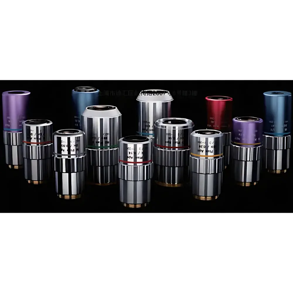
Mitutoyo Wideband Achromatic Objective (UV–NIR)
| Brand | Auniontech |
|---|---|
| Origin | Shanghai, China |
| Manufacturer Type | Authorized Distributor |
| Regional Category | Domestic (China) |
| Model | Wideband Objective |
| Component Category | Optical Element |
| Spectral Range | 200–1800 nm |
| Correction Type | Infinity-Corrected, Plan Apochromatic |
| Working Distance | Long to Extra-Long (varies by series) |
| Customization | Available for substrate thickness (e.g., 0.7 mm, 1.1 mm, 3.5 mm BK7) and refractive index |
Overview
The Mitutoyo Wideband Achromatic Objective (UV–NIR) is an engineered optical component designed for high-fidelity imaging and precision laser manipulation across an exceptionally broad spectral range—from deep ultraviolet (200 nm) through visible light to near-infrared (1800 nm). Unlike conventional visible-light objectives, these objectives employ multi-layer, low-absorption fused silica and calcium fluoride lens elements combined with advanced broadband anti-reflection coatings optimized for minimal wavefront distortion and chromatic aberration correction over the full operational bandwidth. The design adheres to infinity-corrected optical architecture, enabling seamless integration into standard microscope stands, laser scanning systems, and automated inspection platforms. Each series—NUV, VIS, and NIR—is optimized for specific application constraints: NUV variants correct for 355 nm laser lines and broadband UV–VIS imaging; VIS models deliver exceptional color fidelity for metrology and semiconductor inspection; NIR versions maintain diffraction-limited performance up to 1800 nm, supporting applications such as silicon wafer inspection and thermographic microscopy.
Key Features
- Infinity-corrected plan apochromatic design ensures flat field imaging and minimal axial chromatic shift across the entire 200–1800 nm spectrum.
- Three dedicated correction families: M Plan Apo NUV (UV–VIS), M Plan Apo NIR (VIS–NIR), and LCD Plan Apo variants (optimized for transmission through defined glass substrates).
- High-resolution (HR) variants provide ≥50% improvement in modulation transfer function (MTF) at Nyquist frequency compared to standard models, verified per ISO 10110–5 standards.
- Extended working distances (WD): Ranging from 10 mm (M Plan Apo NUV) to >34 mm (LCD Plan Apo NIR HR), facilitating non-contact inspection of sensitive or encapsulated samples.
- Custom substrate compensation: Objectives can be optimized for user-specified cover glass thickness (e.g., 0.7 mm, 1.1 mm, 3.5 mm) and material dispersion (BK7, fused silica, sapphire), ensuring optimal focus and Strehl ratio when imaging through interfaces.
- Robust mechanical construction with black-anodized aluminum housings, parfocal alignment (45 mm reference), and DIN-standard RMS threading (M26×0.707) for interchangeability.
Sample Compatibility & Compliance
These objectives are routinely deployed in GLP-compliant semiconductor metrology labs, ISO 17025-accredited calibration facilities, and FDA-regulated medical device R&D environments. Their broadband correction supports standardized test methods including ASTM E284 (terminology for optics), ISO 10110 (specification of optical components), and JIS B 7152 (microscope objective testing). When integrated into automated inspection systems, they comply with IEC 61000-6-3 (EMC emission requirements) and meet RoHS 3 and REACH substance restrictions. For laser processing applications, all NUV/NIR models are rated for continuous-wave and pulsed irradiation up to 10 W/cm² at 355 nm and 5 kW/cm² at 1064 nm (per ISO 21254 damage threshold testing).
Software & Data Management
While the objective itself is a passive optical element, its performance is fully characterizable via industry-standard metrology software suites—including Zemax OpticStudio (for ray-trace validation), MATLAB-based MTF analysis toolkits, and Metrology Studio (for automated resolution verification per ISO 19038). Objective-specific Zemax prescription files and spot diagram datasets are provided upon request for system-level optical modeling. All calibration reports include traceable wavefront error maps (RMS ≤ λ/10 @ 633 nm), lateral color data (≤0.5 µm over 200–1000 nm), and axial color curves referenced to NIST-traceable interferometric measurements.
Applications
- UV lithography mask inspection using 248 nm or 365 nm illumination.
- High-magnification defect detection on OLED and TFT-LCD panels through 0.7–1.1 mm cover glass.
- NIR reflectance imaging of silicon wafers and compound semiconductor substrates (InP, GaAs) at 1310 nm and 1550 nm.
- Laser micromachining alignment and real-time process monitoring with 355 nm, 532 nm, and 1064 nm sources.
- Confocal Raman spectroscopy requiring uniform throughput from 250 cm⁻¹ to 3500 cm⁻¹ (corresponding to ~785–532 nm excitation).
- Automated optical inspection (AOI) in GMP-compliant medical device manufacturing, where spectral stability across UV–NIR enables multi-modal defect classification.
FAQ
Are these objectives compatible with standard Nikon or Olympus microscope bodies?
Yes—all models use standardized RMS threading (M26×0.707) and are mechanically parfocal with 45 mm tube lens distance, ensuring compatibility with major OEM microscope platforms when paired with appropriate tube lenses.
Can I request custom coating for a specific laser line not listed in the standard portfolio?
Yes. Auniontech offers bespoke AR coating design and deposition services, including dual-band (e.g., 355/1064 nm) and ultra-broadband (200–2000 nm) options, subject to minimum order quantity and lead time.
Do you provide ISO 17025-certified calibration reports?
Calibration reports with uncertainty budgets are available upon request; full ISO/IEC 17025 accreditation is provided through third-party laboratories accredited by CNAS (China National Accreditation Service) or UKAS.
What is the maximum permissible incident angle for oblique illumination setups?
For optimal performance, incident angles should remain ≤5° off-axis; beyond this, coma and field curvature increase measurably—Zemax modeling support is available for off-axis configuration validation.
Is thermal drift characterized over operating temperature ranges?
Yes. All HR-series objectives include thermal expansion coefficient matching between lens elements and housing; focal shift is specified as ≤0.8 µm/°C over 15–35°C ambient range, measured per ISO 10110–10.


