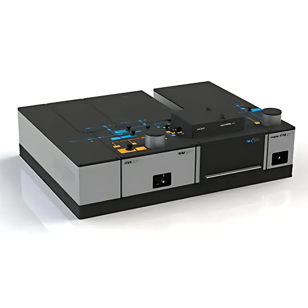
Neaspec neaSNOM Third-Generation Scattering-Type Scanning Near-Field Optical Microscope
| Brand | Neaspec |
|---|---|
| Origin | Germany |
| Model | neaSNOM |
| Application Range | Visible to THz |
| Spatial Resolution | <10 nm |
| Detection Method | Pseudo-Heterodyne Interferometric s-SNOM |
| Compatible Modes | nano-FTIR, TERS, Ultrafast Spectroscopy, THz Imaging |
Overview
The Neaspec neaSNOM is a third-generation scattering-type scanning near-field optical microscope (s-SNOM) engineered for quantitative, label-free nanoscale optical imaging and spectroscopy across the visible, mid-infrared (MIR), and terahertz (THz) spectral ranges. Unlike conventional far-field optical microscopy—limited by the diffraction barrier (~λ/2)—the neaSNOM operates on the principle of scattering-type near-field probing: a sharp metallic atomic force microscope (AFM) tip locally enhances and scatters incident light, generating evanescent fields with sub-10 nm spatial confinement. This mechanism decouples spatial resolution from illumination wavelength, enabling true nanoscale optical contrast independent of photon energy. The system integrates a high-stability AFM platform with interferometric pseudo-heterodyne detection, allowing simultaneous acquisition of near-field amplitude and phase information with high signal-to-noise ratio (SNR) and exceptional reproducibility. Its design meets the stringent demands of quantitative nanophotonics research, where reliable correlation between topography, local dielectric response, and electronic or vibrational excitations is essential.
Key Features
- Sub-10 nm optical resolution: Achieved via scattering-based near-field excitation and higher-harmonic demodulation (typically at 2nd–4th oscillation harmonics), suppressing far-field background while preserving nanoscale contrast fidelity.
- Pseudo-heterodyne interferometric detection: Enables quantitative retrieval of both near-field amplitude and phase, critical for complex dielectric function mapping and plasmonic mode analysis.
- Broadband optical architecture: Reflective, aberration-corrected optics support seamless integration of tunable lasers, quantum cascade lasers (QCLs), synchrotron IR beams, femtosecond Ti:sapphire systems, and THz sources—without realignment.
- Dual-beam path configuration: Provides 180° horizontal and 60° vertical optical access, facilitating co-linear pump-probe ultrafast experiments, oblique illumination studies, and multi-modal coupling (e.g., simultaneous s-SNOM + TERS).
- High-stability AFM base: Designed for low thermal drift (<0.5 nm/min) and mechanical noise suppression, optimized for long-duration spectroscopic line scans and hyperspectral image acquisition under ambient or controlled environments.
- Modular multimodal expansion: Native compatibility with nano-FTIR, tip-enhanced Raman spectroscopy (TERS), time-resolved ultrafast near-field imaging, and THz near-field detection—enabling correlative nanoscale structure–function analysis.
Sample Compatibility & Compliance
The neaSNOM accommodates standard AFM substrates—including Si/SiO₂ wafers, CaF₂, BaF₂, ZnSe, and conductive ITO/glass—without specialized mounting or vacuum requirements. Samples may be measured in ambient air, inert gas, or temperature-controlled stages (optional cryogenic or heating modules). The system adheres to ISO/IEC 17025 principles for measurement traceability and supports GLP-compliant data recording through timestamped metadata logging, instrument parameter archiving, and user-accessible raw interferogram storage. While not FDA-regulated (as a research instrument), its software architecture aligns with 21 CFR Part 11 expectations for audit trails, electronic signatures, and data integrity—facilitating adoption in regulated academic core facilities and industrial R&D labs engaged in nanomaterial characterization for optoelectronics or pharmaceutical development.
Software & Data Management
neaSCAN software provides an integrated environment for instrument control, real-time feedback, spectral acquisition, and post-processing. It supports automated spectral stitching across multiple laser lines or broadband detectors, FFT-based phase unwrapping, dielectric function inversion (ε = ε′ + iε″) via Kramers–Kronig analysis, and vectorial near-field field reconstruction. All datasets are stored in HDF5 format with embedded metadata (wavelength, demodulation order, tip geometry, environmental conditions), ensuring FAIR (Findable, Accessible, Interoperable, Reusable) compliance. Batch processing pipelines enable high-throughput analysis of large hyperspectral cubes (>10⁶ pixels), and Python/C++ APIs allow integration with custom machine learning workflows for pattern recognition in nanoscale infrared heterogeneity or plasmon dispersion mapping.
Applications
- Nanoscale mapping of plasmon polaritons in graphene, doped semiconductors, and hyperbolic metamaterials
- Vibrational nano-spectroscopy (nano-FTIR) of polymer blends, biological membranes, and 2D material heterostructures
- Carrier dynamics and exciton transport in transition metal dichalcogenides (TMDs) and perovskite nanocrystals
- Phonon–plasmon coupling in vanadium dioxide (VO₂) phase-transition materials
- Tip-enhanced Raman spectroscopy (TERS) of catalytic surfaces and single-molecule adsorbates
- Ultrafast near-field pump–probe imaging of hot-carrier relaxation and coherent phonon generation
- Terahertz near-field imaging of carrier screening, domain walls, and topological edge states
FAQ
What spectral ranges does the neaSNOM support?
The system is fully compatible with visible (400–700 nm), mid-infrared (2.5–20 µm), and terahertz (1–10 THz) radiation sources, enabled by its all-reflective optical design.
Is vacuum operation required?
No—measurements are routinely performed in ambient air; optional environmental chambers support controlled humidity, inert gas, or low-temperature operation.
Can the neaSNOM perform quantitative dielectric imaging?
Yes—interferometric detection enables retrieval of both amplitude and phase of the near-field signal, permitting direct calculation of local complex permittivity using established inversion models.
How is tip calibration handled?
Tip geometry is characterized ex situ via SEM, and tip-induced field enhancement is modeled using boundary element method (BEM) simulations; standardized reference samples (e.g., SiO₂-on-Si gratings) are used for routine sensitivity validation.
Is training and application support available?
Neaspec provides on-site installation, comprehensive operator training, and ongoing remote technical support—including assistance with experimental design, data interpretation, and publication-ready figure generation.


