NIPPON KAYAKU KPM-500 DFR Permanent Negative-Tone Dry Film Photoresist for Wafer Bonding
| Brand | NIPPON FILCON |
|---|---|
| Origin | Japan |
| Manufacturer Type | Authorized Distributor |
| Origin Category | Imported |
| Model | NIPPON KAYAKU KPM-500 DFR |
| Pricing | Upon Request |
Overview
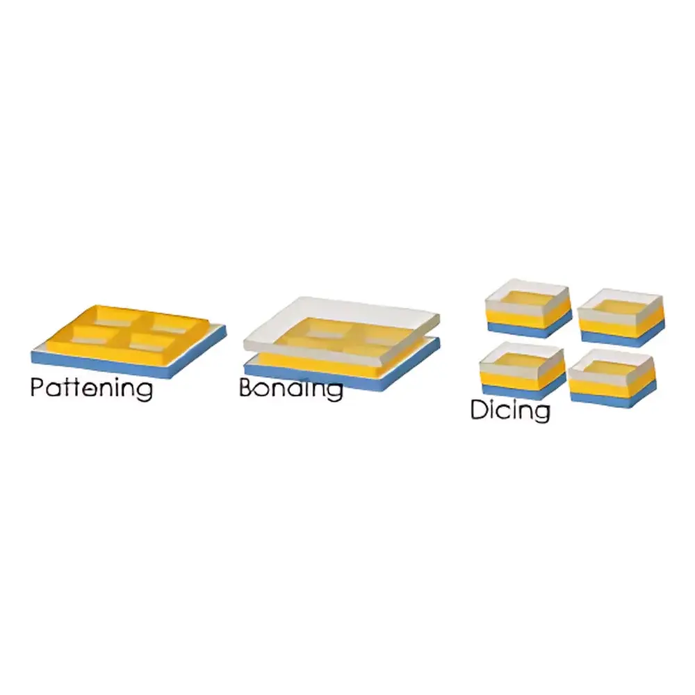
The NIPPON KAYAKU KPM-500 DFR is a high-performance, permanent negative-tone dry film photoresist engineered specifically for advanced wafer-level bonding applications in MEMS, sensor packaging, and microfluidic device fabrication. Unlike conventional temporary bonding materials or spin-coated resists, KPM-500 DFR is supplied as a solvent-free, laminated dry film—enabling uniform thickness control (typically 10–50 µm), minimal outgassing, and exceptional process reproducibility. Its photoreaction mechanism relies on cationic polymerization initiated by deep-UV (i-line, 365 nm) or broadband exposure, followed by thermal post-exposure bake (PEB) and full cure at 180 °C. The resulting crosslinked network exhibits high chemical resistance to standard semiconductor wet etchants (e.g., KOH, TMAH, HF-based solutions) and sustained mechanical integrity under thermal cycling (−40 °C to +250 °C), making it suitable for hermetic cavity formation and structural encapsulation.
Key Features
- Halogen-free, antimony-free formulation compliant with JEDEC J-STD-020 and RoHS 3 directives
- Water-developable using aqueous tetramethylammonium hydroxide (TMAH) at 0.26 N concentration—eliminating need for organic solvents and reducing environmental and safety burden
- High adhesion strength (>15 MPa) to silicon, fused silica, quartz, and low-κ dielectrics after full cure; validated via pull-test and tape peel per ASTM D3359
- Low-temperature bonding capability: void-free wafer bonding achieved at 150 °C under 10.2 kN applied force (equivalent to ~1.5 MPa pressure)
- High-resolution patterning: supports sub-5 µm line/space features with vertical sidewalls (aspect ratio >3 at 20 µm thickness) when exposed with i-line steppers or mask aligners
- Thermal stability up to 250 °C post-cure; coefficient of thermal expansion (CTE) matched closely to silicon (≈3.5 ppm/°C)
Sample Compatibility & Compliance
KPM-500 DFR demonstrates broad compatibility across front-end and back-end semiconductor substrates—including bare Si wafers (200 mm and 300 mm), SOI, glass carriers (e.g., Borofloat 33, Eagle XG), and thin-film metallized surfaces (Al, Cu, TiW). It has been qualified for use in cleanroom environments meeting ISO Class 5 (Class 100) standards and is compatible with standard wafer handling equipment (FOUPs, EFEMs, laminators, and exposure tools). Material composition complies with IPC-4101D for base laminate materials and meets halogen content limits per IEC 61249-2-21 (<900 ppm Cl, <900 ppm Br, total halogens <1500 ppm). Lot-to-lot consistency is ensured through NIPPON KAYAKU’s ISO 9001-certified manufacturing and traceability per lot number, including full Certificate of Analysis (CoA) and Certificate of Conformance (CoC).
Software & Data Management
As a material—not an instrument—KPM-500 DFR does not include embedded software or firmware. However, its process integration is fully supported by industry-standard lithography recipe management systems (e.g., ASML YieldStar, Nikon NSR-S630D, EVG Gemini® bond aligner platforms). Process parameters—including lamination temperature/pressure profiles, exposure dose (mJ/cm²), PEB ramp rates, and cure cycles—are documented in NIPPON KAYAKU’s Technical Data Sheet (TDS) and Process Integration Guide (PIG), both available in English and aligned with SEMI E10 (Specification for Definition and Measurement of Equipment Reliability, Maintainability, and Availability) and SEMI E142 (Guideline for Traceability of Semiconductor Manufacturing Materials). For GMP/GLP-regulated environments (e.g., medical MEMS or automotive-grade sensors), full audit trails for material lot release, shelf-life tracking (24 months unopened at 5–25 °C), and retest intervals are maintained per internal QA protocols and FDA 21 CFR Part 11-compliant documentation practices.
Applications
- Wafer-level cavity sealing for SAW/BAW filters, pressure sensors, and inertial MEMS devices
- Structural bonding layers in 3D heterogeneous integration (e.g., chip stacking, interposer bonding)
- Microfluidic channel capping and reservoir encapsulation with long-term fluid compatibility (tested vs. DI water, ethanol, PBS, and 10% NaOH)
- Temporary carrier bonding/debonding processes where low-stress delamination is required (e.g., thin-wafer handling during TSV processing)
- Passivation and etch mask layers in RF-MEMS and optical MEMS fabrication flows
FAQ
What is the recommended lamination temperature and pressure for KPM-500 DFR?
Lamination is performed at 80–100 °C with roll pressure of 0.3–0.5 MPa for 1–2 m/min web speed; optimal adhesion is achieved with pre-bake at 90 °C for 5 min prior to exposure.
Is KPM-500 DFR compatible with plasma ashing or oxygen RIE?
Yes—it withstands standard O₂ plasma descum (100–200 W, 100–300 mTorr, 60–120 sec) without edge lifting or residue formation; full removal requires extended O₂/CF₄ chemistry at elevated power.
Does the material require humidity-controlled storage?
Yes—store unopened rolls at 5–25 °C with relative humidity <50%; desiccant packs are included in original packaging to prevent moisture uptake prior to lamination.
Can KPM-500 DFR be used for through-silicon via (TSV) insulation?
While not optimized as a primary TSV liner, it has demonstrated dielectric strength >5 MV/cm and volume resistivity >1×10¹⁵ Ω·cm post-cure—making it suitable for secondary insulation or planarization layers adjacent to TSV structures.
What is the shelf life after opening the package?
Once opened, use within 72 hours under nitrogen-purged environment (dew point <−40 °C); extended handling requires resealing with vacuum desiccation and cold storage at 5 °C.


