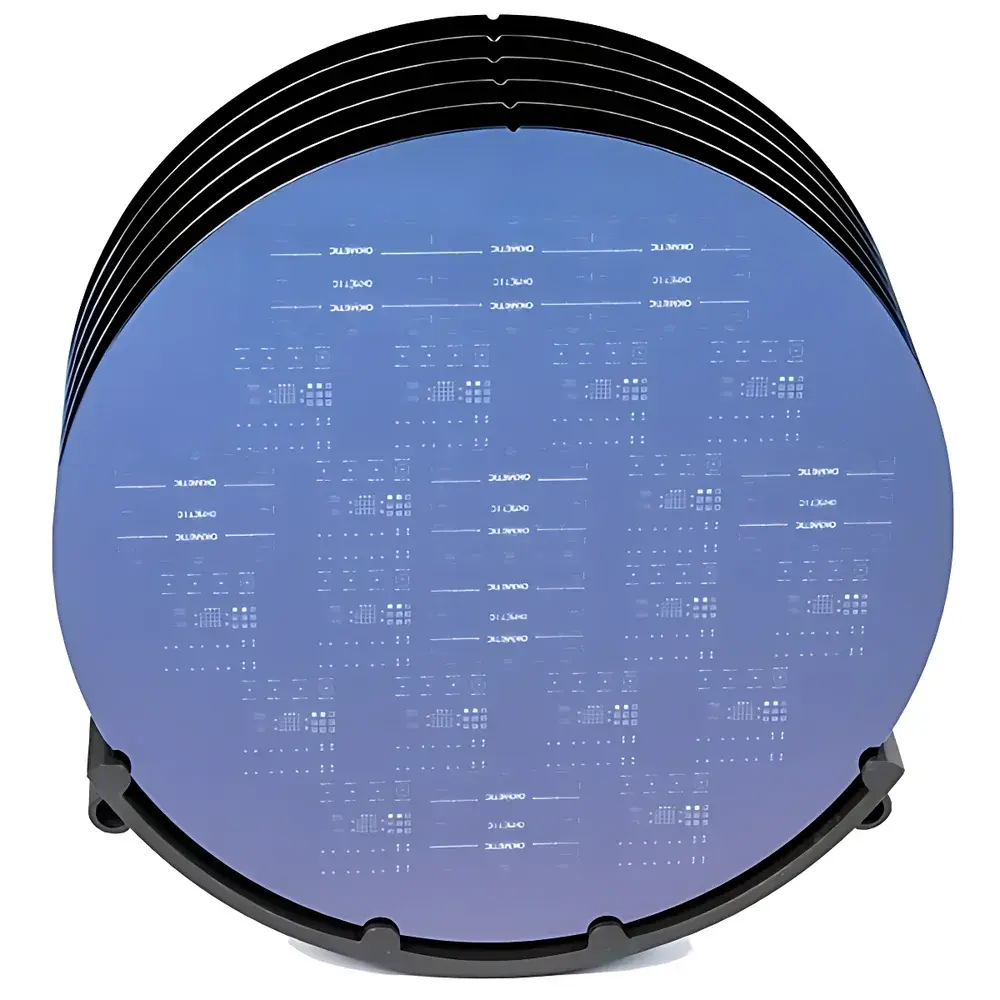
Okmetic SOI Silicon Wafers for Microfluidic Chip Fabrication
| Brand | Okmetic |
|---|---|
| Origin | Finland |
| Wafer Type | SOI (Silicon-on-Insulator) |
| Substrate Material | Single-Crystal Silicon |
| Structural Configuration | Handle Layer / Buried Oxide (BOX) / Device Layer |
| Available Formats | Prime, Double-Side Polished (DSP), Patterned Device Layer Options |
| Process Compatibility | MEMS, Deep Reactive Ion Etching (DRIE), Anodic Bonding, Wafer-Level Sealing |
| Resistivity Range | 0.001–10,000 Ω·cm |
| Device Layer Thickness | 1–50 µm (customizable) |
| BOX Thickness | 0.1–4 µm (customizable) |
| Diameter Options | 100 mm, 150 mm, 200 mm |
| Surface Roughness (Ra) | <0.2 nm (prime/DSP) |
Overview
Okmetic SOI silicon wafers are engineered substrates specifically designed for high-precision microfabrication of microfluidic chips, lab-on-a-chip (LoC) systems, and integrated MEMS-based biosensors. Built upon the Silicon-on-Insulator architecture, each wafer consists of three structurally defined layers: a mechanical support handle wafer, a thermally grown or deposited buried oxide (BOX) layer serving as both electrical isolation and etch-stop barrier, and a top device layer of single-crystal silicon—typically 1–50 µm thick—where microchannels, electrodes, transducers, and functional microstructures are patterned via photolithography and deep reactive ion etching (DRIE). The BOX layer’s uniform thickness and dielectric integrity enable precise control over membrane deflection, capacitive sensing gaps, and electrostatic actuation—critical parameters in pressure sensors, flow meters, and droplet-based digital microfluidics. Manufactured in ISO 9001- and IATF 16949-certified cleanrooms in Finland, Okmetic’s SOI wafers meet stringent requirements for surface flatness (<0.2 nm Ra), thickness uniformity (≤±1.5% TTV), and crystallographic orientation (e.g., <100>, <110>, or <111>), ensuring reproducible process integration across academic, clinical diagnostic, and industrial R&D environments.
Key Features
- Proprietary bonding-based SOI fabrication with controlled BOX thickness (0.1–4 µm) and low interface trap density (<1×1011 cm−2eV−1)
- Full spectrum of SOI variants: BSOI (Bonded SOI), C-SOI® (Cavity-SOI), E-SOI® (Enhanced SOI), and RFSi® (Radio-Frequency SOI) optimized for RF-MEMS and high-frequency bioimpedance applications
- Device layer customization: unpatterned prime wafers, pre-patterned microchannel layouts (e.g., serpentine, herringbone, or mixer geometries), and multi-level through-silicon vias (TSVs) for 3D interconnect integration
- Double-side polished (DSP) and single-side polished (SSP) options compliant with SEMI standards; available in 100 mm, 150 mm, and 200 mm diameters
- Controlled resistivity range (0.001–10,000 Ω·cm) supporting both conductive electrode integration and high-impedance sensing configurations
- Traceable lot documentation including XRR (X-ray reflectivity), ellipsometry, and AFM surface characterization reports
Sample Compatibility & Compliance
Okmetic SOI wafers are compatible with standard semiconductor and MEMS processing tools—including stepper lithography, Bosch-process DRIE, thermal oxidation, LPCVD SiN/SiO2, and anodic bonding to Pyrex or glass. Their dimensional stability under thermal cycling (−40°C to +150°C) and chemical resistance to KOH, TMAH, and HF-based etchants make them suitable for wafer-level packaging of sealed microfluidic chambers. All wafers comply with RoHS Directive 2011/65/EU and REACH Regulation (EC) No. 1907/2006. For regulated life science applications, Okmetic provides material traceability down to furnace batch level and supports audit readiness for ISO 13485:2016 and FDA 21 CFR Part 11-compliant documentation workflows.
Software & Data Management
While Okmetic SOI wafers are passive substrates, they integrate seamlessly with industry-standard design and simulation platforms including COMSOL Multiphysics® (for fluid-structure interaction modeling), CoventorWare® (MEMS layout and process simulation), and Cadence Virtuoso® (for co-design of embedded CMOS readout circuitry). Each wafer shipment includes a digital Certificate of Conformance (CoC) with metrology data (thickness mapping, surface roughness, defect scan reports), accessible via Okmetic’s secure customer portal. Raw metrology datasets (CSV, .mat) are available upon request to support GLP/GMP-aligned validation protocols.
Applications
- High-aspect-ratio microchannel fabrication for point-of-care (POC) immunoassay chips and nucleic acid extraction devices
- Capacitive and piezoresistive pressure sensors in ventilator monitoring and wearable physiological monitors
- Electrokinetic pumps and valves in portable drug delivery microsystems
- Optofluidic platforms integrating waveguides and micro-lenses fabricated via selective epitaxy on patterned SOI
- Organ-on-a-chip platforms requiring hermetic sealing and long-term cell viability under perfusion
- RF-MEMS switches and tunable filters for wireless biomedical telemetry modules
FAQ
What is the minimum device layer thickness achievable with Okmetic’s SOI wafers?
Standard device layers start at 1 µm; sub-micron layers (down to 200 nm) are available under custom process agreements with additional qualification.
Can Okmetic provide SOI wafers with pre-fabricated microfluidic channel patterns?
Yes—C-SOI® and patterned E-SOI® wafers include lithographically defined device-layer topographies, including trench depths up to 80% of the device layer thickness, with sidewall angles >85°.
Is BOX layer thickness uniformity guaranteed across the wafer?
Yes—Okmetic specifies BOX thickness non-uniformity ≤±2.5% across 100 mm wafers and ≤±3.0% across 200 mm wafers, verified by spectroscopic ellipsometry and XRR.
Do you offer technical support for process integration?
Yes—Okmetic’s application engineers provide confidential process compatibility assessments, DRIE parameter recommendations, and bonding yield optimization guidance, supported by documented case studies from academic and industrial partners.
Are material safety data sheets (MSDS) and RoHS declarations available?
Yes—all documentation is accessible via the Okmetic Customer Portal upon registration and is updated per EU regulatory revisions.