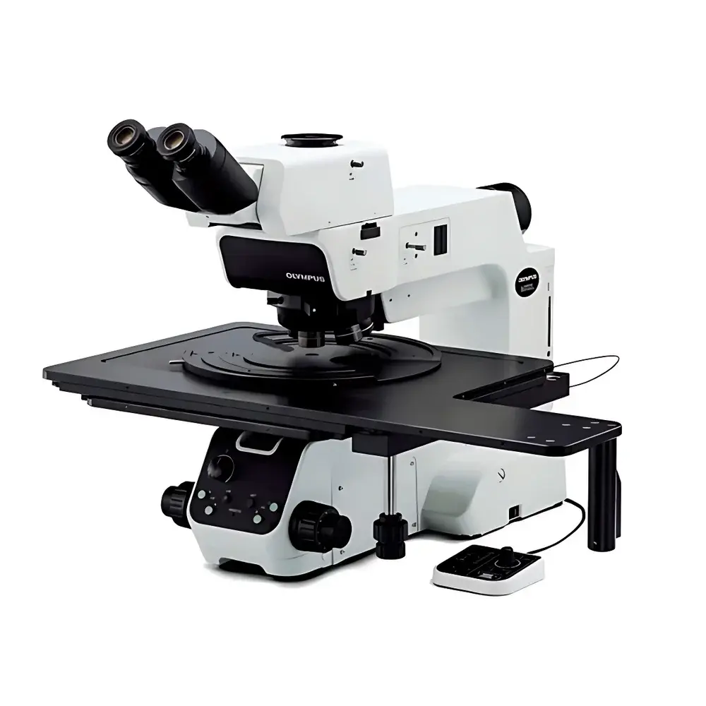
OLYMPUS MX63L Semiconductor Industrial Inspection Microscope
| Brand | OLYMPUS |
|---|---|
| Origin | Japan |
| Model | MX63L |
| Application | Wafer, FPD, PCB, and Large-Scale Component Inspection |
| Compliance | SEMI S2/S8, CE, UL |
| Modular Architecture | Yes |
| Software Platform | Olympus Stream Imaging & Analysis Suite |
| Optional Automation | AL120 Wafer Handler (200 mm), Motorized Z-Stage, DP22/DP27 Digital Cameras |
Overview
The OLYMPUS MX63L Semiconductor Industrial Inspection Microscope is a high-precision, modular optical inspection system engineered for non-destructive macro- and micro-scale evaluation of large-format semiconductor substrates—including 150 mm to 300 mm silicon wafers, compound semiconductor wafers, flat panel displays (FPDs), printed circuit boards (PCBs), and advanced packaging components. Built upon a rigid, vibration-damped mechanical platform, the MX63L employs Köhler illumination principles combined with interchangeable objective turrets and a wide-field optical path optimized for high-resolution, low-distortion imaging across extended working distances. Its core architecture supports both manual and motorized operation modes, enabling seamless transition between rapid visual screening and metrologically traceable quantitative analysis. Designed specifically for cleanroom-integrated environments, the system minimizes particle generation and electrostatic discharge (ESD) risk through fully shielded electronics, anti-static surface treatments on all optical and mechanical components, and sealed motor housings—ensuring compatibility with ISO Class 5 (Class 100) or stricter cleanroom classifications per SEMI S2/S8 safety and environmental guidelines.
Key Features
- Modular optical configuration supporting brightfield, darkfield, differential interference contrast (DIC), polarized light, and fluorescence observation methods—enabling defect detection across diverse material types and surface conditions.
- MIX Observation Technology: Integrates segmented quadrant-controlled LED darkfield illumination with simultaneous brightfield or polarized channels to enhance edge contrast, reveal subsurface scattering anomalies, and visualize topographic features invisible under conventional illumination.
- Extended Focus Imaging (EFI): Acquires z-stack image sequences via manual or motorized Z-axis control; reconstructs artifact-free, depth-of-field-extended composite images for height-resolved structural assessment—critical for bump inspection, trench profiling, and die-level morphology analysis.
- Multi-Image Acquisition (MIA): Enables rapid panoramic stitching using pattern-matching algorithms within Olympus Stream software—no motorized stage required; ideal for full-wafer mapping and defect localization across 300 mm substrates.
- High Dynamic Range (HDR) Image Capture: Compensates for localized overexposure and shadowing in heterogeneous samples (e.g., metallized traces adjacent to dielectric layers), preserving detail in both highlight and low-light regions without post-processing artifacts.
- Ergonomic design with tilting binocular observation tube, low-profile stage controls, and integrated clutch mechanism for XY-stage coarse/fine motion—reducing operator fatigue during prolonged inspection shifts.
Sample Compatibility & Compliance
The MX63L accommodates wafer diameters from 75 mm to 300 mm using interchangeable stage inserts and carrier plates—supporting standard SEMI-compliant cassette formats (e.g., FOUP, SMIF). Optional AL120 automated wafer handler enables tool-free, ESD-safe transfer of 200 mm wafers directly from front-opening unified pods (FOUPs) to the inspection stage, eliminating manual handling-induced contamination and mechanical damage. All electrical subsystems are housed within sealed enclosures conforming to IEC 61000-6-2 (immunity) and IEC 61000-6-4 (emission) standards. The system meets SEMI S2 (safety) and S8 (ergonomics) requirements, carries CE marking under the EU Machinery Directive 2006/42/EC and Low Voltage Directive 2014/35/EU, and complies with UL 61010-1 for laboratory equipment safety.
Software & Data Management
Olympus Stream desktop software serves as the central hub for acquisition, measurement, analysis, and reporting. It supports FDA 21 CFR Part 11–compliant audit trails when configured with user authentication and electronic signature modules—fulfilling GLP/GMP documentation requirements for regulated semiconductor manufacturing environments. Measurement data—including length, area, angle, particle count, and profile roughness—is embedded directly into image metadata and exported alongside annotated TIFF/PNG files. Predefined report templates generate Microsoft Word and PowerPoint-compatible documents with embedded zoomable images, scale bars, and calibrated measurements—ensuring traceability and reproducibility across QA/QC workflows. Offline EFI reconstruction and batch MIA processing allow computational tasks to be decoupled from real-time inspection, optimizing throughput in high-volume production labs.
Applications
- Front- and backside macro-inspection of silicon and GaAs wafers for particle contamination, scratches, chipping, and coating uniformity.
- Defect classification and root-cause analysis in lithography, etch, deposition, and CMP process steps.
- Qualitative and semi-quantitative assessment of solder bumps, redistribution layers (RDL), and through-silicon vias (TSVs) in advanced packaging.
- Visual verification of alignment marks, fiducials, and mask registration accuracy on photomasks and reticles.
- Non-contact dimensional verification of PCB traces, solder paste volume estimation, and component placement accuracy.
- Material characterization of thin-film stacks, crystallinity indicators, and stress-induced cracking in optoelectronic devices.
FAQ
Does the MX63L support automated wafer handling?
Yes—the optional AL120 wafer handler integrates seamlessly with the MX63L platform for hands-free, ESD-safe loading/unloading of 200 mm wafers from standard FOUPs.
Can EFI and MIA be performed without motorized stages?
EFI requires precise Z-axis movement and is compatible with both manual micrometer drives and motorized Z-stages; MIA operates effectively with manual XY-stage navigation using Olympus Stream’s real-time pattern recognition.
Is Olympus Stream software validated for regulated environments?
When deployed with enabled audit trail, role-based access control, and electronic signatures, Olympus Stream meets FDA 21 CFR Part 11 and ISO/IEC 17025 documentation integrity requirements.
What camera models are natively supported?
The MX63L is fully compatible with Olympus DP22 (2.0 MP) and DP27 (5.9 MP) digital microscope cameras, offering USB 3.0 connectivity, low-noise CMOS sensors, and hardware-triggered capture synchronization.
How does the MX63L minimize contamination in cleanroom settings?
All motors are enclosed in dust-tight housings, surfaces undergo anti-static coating (surface resistivity <1×10⁹ Ω/sq), airflow paths avoid direct exposure to optics, and the entire system passes SEMI S2 particle emission testing protocols.


