Oxford Instruments AZtecWave WDS System for SEM
| Brand | Oxford Instruments |
|---|---|
| Origin | United Kingdom |
| Model | AZtecWave |
| Detector Type | Wavelength Dispersive Spectrometer (WDS) with Integrated EDS Compatibility (Ultim Max) |
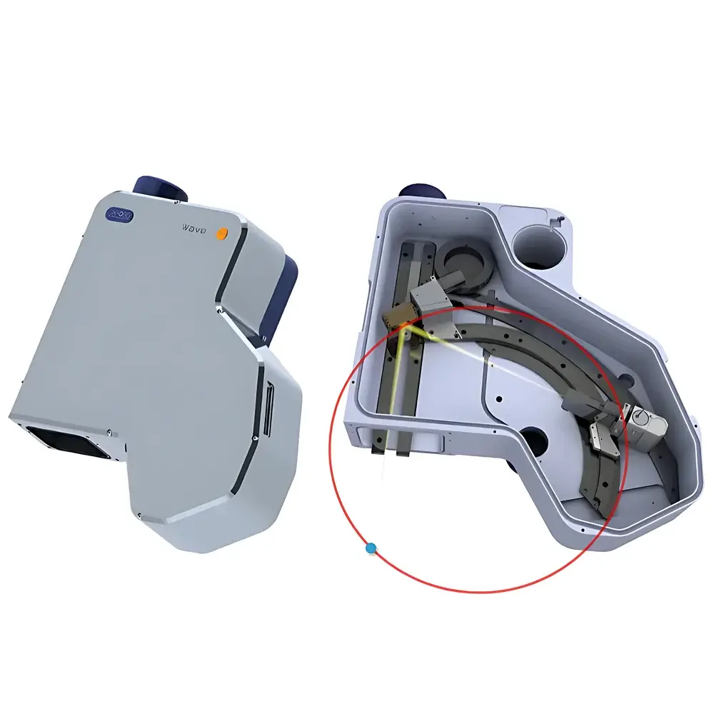
| Roland Circle Radius | 210 mm |
| Energy Resolution | <10 eV (Mn Kα, typical) |
| Detection Limit | <100 ppm (matrix-dependent) |
| Peak-to-Background Ratio | >10,000:1 (typical for major elements) |
| Optical Geometry | Focusing Johann-type spectrometer with bent crystals |
| Incident Slit | Motorized, variable width |
| Installation | Tilt-mounted for minimal working distance dependency |
| Software Platform | AZtecWave v4.x or later |
Overview
The Oxford Instruments AZtecWave Wavelength Dispersive Spectrometer (WDS) is a high-performance microanalysis add-on system engineered for integration with scanning electron microscopes (SEM). It delivers quantitative elemental analysis at trace and ultra-trace levels—down to sub-100 ppm detection limits—by exploiting the fundamental principles of Bragg diffraction. Unlike energy-dispersive spectroscopy (EDS), which measures X-ray photon energies directly, WDS disperses characteristic X-rays using precisely curved single-crystal analyzers mounted on a fixed-radius (210 mm) Johann-type focusing geometry. This architecture enables exceptional spectral resolution (<10 eV at Mn Kα), allowing unambiguous separation of overlapping peaks (e.g., S Kα/Pb Mα, Ti Kβ/V Kα, or rare-earth L-lines), which are routinely unresolved in conventional EDS systems. AZtecWave is not a standalone instrument but a modular, vacuum-compatible WDS platform designed to operate in parallel with Oxford’s Ultim Max silicon drift detector (SDD), enabling hybrid EDS/WDS workflows: rapid survey mapping via EDS followed by targeted, high-accuracy quantification via WDS.
Key Features
- Focusing Johann geometry with 210 mm Roland circle radius ensures optimal X-ray collection efficiency and intrinsic energy resolution.
- Bent LiF(200), PET, TAP, and LDE crystals provide full coverage from Be (48 eV) to U (13.6 keV), with selectable crystal exchange under vacuum.
- Tilt-mounted spectrometer design decouples X-ray intensity from working distance variations—critical for topographic or tilted-sample analyses.
- Motorized incident slit (5–200 µm width) allows real-time optimization of spectral resolution versus count rate, balancing detection limit and acquisition speed.
- High peak-to-background ratio (>10,000:1 for major elements) minimizes matrix correction uncertainty and improves accuracy for light elements (Z < 11) and low-concentration species.
- Integrated thermal and mechanical stabilization maintains long-term calibration stability—essential for multi-hour quantitative sessions and inter-laboratory reproducibility.
Sample Compatibility & Compliance
AZtecWave supports standard SEM-compatible sample geometries up to 100 mm diameter and 50 mm height, including bulk metals, ceramics, geological thin sections, polished cross-sections, and coated insulators (with appropriate charge compensation). The system complies with IEC 61000-6-3 (EMC emission standards) and meets CE marking requirements for laboratory instrumentation. All quantitative routines adhere to ISO 14707:2005 (electron probe microanalysis—quantitative analysis using wavelength dispersive spectrometry) and ASTM E1508–19 (standard guide for quantitative elemental analysis by WDS). Data acquisition and processing workflows support audit trails, electronic signatures, and user-access controls aligned with FDA 21 CFR Part 11 and GLP/GMP documentation frameworks when deployed in regulated QA/QC environments.
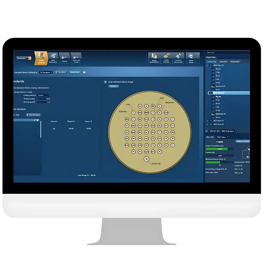
Software & Data Management
AZtecWave operates within the unified AZtec platform (v4.5+), providing synchronized control of both WDS and EDS detectors. The software features guided workflow wizards—including automated peak identification, interference correction setup, and ZAF/φ(ρz) matrix correction selection—enabling novice users to perform rigorous WDS quantification without deep spectroscopic expertise. All spectra, maps, and quantification reports are stored in vendor-neutral HDF5 format with embedded metadata (beam kV, current, dwell time, crystal type, slit width, background model). Batch processing, scriptable macros (Python API), and export to CSV, Excel, or CMA-ES-compatible formats facilitate integration into LIMS and statistical process control (SPC) pipelines. Raw spectral data retains full channel-level fidelity for retrospective reprocessing or method validation.
Applications
AZtecWave is routinely deployed in materials science laboratories for phase-specific chemistry in multiphase alloys (e.g., γ/γ′ in Ni-superalloys), oxidation state differentiation in transition metal oxides (e.g., Fe²⁺/Fe³⁺ partitioning in spinels), and trace contaminant profiling in semiconductor gate dielectrics (<5 nm SiO₂ layers). In geosciences, it enables precise REE (rare earth element) fractionation studies in zircon and monazite via L-line WDS, circumventing EDS overlaps. Forensic labs apply it to gunshot residue (GSR) particle characterization where Pb/Sb/Ba ratios must be resolved below 200 ppm; metallurgical QA uses it for inclusion chemistry in bearing steels per ISO 4967. Its ability to quantify light elements (C, N, O) in nitrides and carbides—without helium purge—makes it indispensable for advanced ceramic R&D.
FAQ
How does AZtecWave differ from conventional EDS-only systems in terms of analytical capability?
AZtecWave achieves ~10× better energy resolution than EDS, enabling definitive identification and quantification of elements with overlapping X-ray lines—especially critical for adjacent atomic numbers (e.g., V/Ti, S/Pb, or lanthanide series) and light-element analysis where peak broadening dominates EDS spectra.
Can AZtecWave be retrofitted onto existing SEM platforms?
Yes—AZtecWave is compatible with major SEM manufacturers (Thermo Fisher Scientific, Zeiss, JEOL, Hitachi) via standardized flange interfaces (CF100 or CF160) and digital communication protocols (Ethernet/IP, RS-232). Oxford Instruments provides mechanical integration kits and beam-parameter synchronization modules.
What maintenance is required for long-term WDS performance?
Annual crystal cleanliness verification and vacuum integrity checks are recommended. Crystal aging is negligible under normal operation; no routine recalibration is needed unless mechanical shock or thermal cycling exceeds specification limits.
Is AZtecWave compliant with regulatory documentation requirements for pharmaceutical or medical device manufacturing?
When configured with AZtec’s optional Audit Trail and User Access Control modules, the system satisfies FDA 21 CFR Part 11 and EU Annex 11 requirements for electronic records and signatures in GxP environments.


