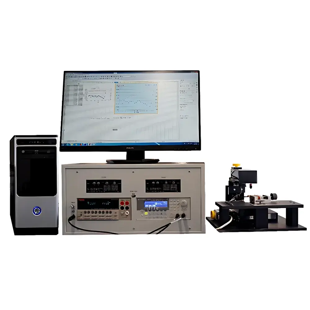
Panco PSM II Conductivity–Seebeck Coefficient Scanning Probe Microscope
| Brand | Panco |
|---|---|
| Origin | Germany |
| Model | PSM II |
| Positioning Accuracy | Unidirectional 0.05 µm |
| Maximum Scan Area | 100 mm × 100 mm (typ.) |
| Local Measurement Resolution | 5 µm |
| Voltage Measurement Sensitivity | 100 nV |
| Seebeck Coefficient Measurement Uncertainty | < 3% (semiconductors), < 5% (metals) |
| Electrical Conductivity Measurement Uncertainty | < 4% |
| Point Acquisition Time | 4–20 s per measurement |
| Repeatability Error | < 3% |
| System Configuration | Triaxial precision positioning stage, force-sensing contact probe, integrated heating/temperature-sensing probe, analog multiplexer, 6½-digit digital voltmeter, lock-in amplifier, coaxial optical imaging module, dedicated control software with API support for LabVIEW and Python |
Overview
The Panco PSM II Conductivity–Seebeck Coefficient Scanning Probe Microscope is a purpose-built, research-grade instrument engineered for spatially resolved thermoelectric property mapping at the microscale. Unlike conventional bulk thermoelectric characterization systems, the PSM II operates on the principle of localized four-point probe thermovoltage measurement combined with simultaneous electrical resistance profiling—enabling concurrent, co-registered quantification of both Seebeck coefficient (S) and electrical conductivity (σ) across heterogeneous surfaces. The system implements a calibrated thermal gradient (typically 1–5 K/mm) generated via a micro-heater-integrated probe tip, while a second thermally isolated voltage-sensing tip measures the resulting thermoelectromotive force. This dual-tip, differential configuration eliminates parasitic thermal EMFs and ensures traceable S values in accordance with ISO 8502-2 and ASTM E1577–22 guidelines for thermoelectric material evaluation. Designed in collaboration with the German Aerospace Center (DLR), the PSM II delivers nanoscale mechanical stability and sub-micron positional fidelity—critical for resolving grain-boundary effects, phase segregation, and interfacial transport anomalies in advanced thermoelectrics.
Key Features
- First commercially available SPM platform capable of quantitative, pixel-by-pixel Seebeck coefficient mapping—fully decoupled from topographic artifacts
- Active force-feedback probe contact control ensures consistent normal load (1–50 mN adjustable) and minimizes sample deformation during scanning on soft or brittle materials (e.g., Bi2Te3-based thin films)
- Dual-channel lock-in detection architecture (SR830-class equivalent) with 100 nV RMS sensitivity and 120 dB dynamic reserve enables high-SNR thermovoltage acquisition under ambient or controlled-atmosphere conditions
- Triaxial piezoelectric stage with closed-loop capacitive position sensing achieves unidirectional repeatability of ±0.05 µm and bidirectional hysteresis < 0.1 µm over full 100 mm × 100 mm travel range
- Integrated coaxial optical microscope (10×–50× magnification, motorized focus) allows real-time visual alignment of probe positions relative to microstructural features (grains, cracks, electrodes)
- Modular electronics architecture supports future expansion: optional cryogenic sample stage (4–300 K), vacuum-compatible chamber (<10−5 mbar), or electrochemical cell integration
Sample Compatibility & Compliance
The PSM II accommodates solid-state specimens ranging from polished bulk ingots (diameter ≤ 50 mm, thickness ≥ 0.5 mm) to freestanding thin films (≥ 50 nm thick) on insulating or conductive substrates. No metallization or electrode patterning is required—measurements are performed directly on as-prepared surfaces. The system complies with IEC 61000-4-3 (EMC immunity), CE machinery directive 2006/42/EC, and meets mechanical safety requirements per ISO 12100. All measurement data streams—including raw lock-in outputs, stage coordinates, temperature logs, and contact force traces—are timestamped and stored with full audit trail metadata, satisfying GLP documentation standards and enabling retrospective validation per FDA 21 CFR Part 11 when paired with optional electronic signature modules.
Software & Data Management
Control and analysis are executed via Panco’s proprietary PSM-Studio v4.2 software suite, built on a Qt/C++ framework with native 64-bit multithreading support. The interface provides synchronized real-time visualization of S(x,y), σ(x,y), and dS/dx overlays on optical images. Batch scripting (Python API included) enables automated grid scans, multi-temperature series, and cross-correlation with external XRD or Raman datasets. Export formats include HDF5 (with embedded metadata schema compliant with NeXus standard), CSV, and TIFF stacks compatible with ImageJ/Fiji and MATLAB. Raw voltage and current time-series data are saved in binary format with lossless compression (LZ4), preserving full 24-bit ADC resolution for post-hoc noise spectral analysis.
Applications
- Microscale homogeneity assessment of thermoelectric alloys (e.g., half-Heuslers, skutterudites) and oxide ceramics (Ca3Co4O9, NaxCoO2)
- Quantitative mapping of interfacial Seebeck discontinuities in functionally graded materials (FGMs) and thermoelectric module interconnects
- In situ monitoring of degradation mechanisms—e.g., dopant migration in PbTe or oxidation-induced S reduction in Mg2Si films
- Characterization of contact resistance at metal/semiconductor interfaces (e.g., Ni/Bi2Te3) via spatial derivative analysis of potential profiles
- Correlating local carrier concentration gradients (from σ maps) with lattice strain fields measured by micro-Raman
- Validation of computational models (Boltzmann transport + DFT) requiring experimentally constrained spatial S(μ) and σ(T) inputs
FAQ
Does the PSM II require vacuum operation?
No—measurements are routinely performed in ambient air or inert gas (N2, Ar) environments. Vacuum compatibility is available as an optional upgrade.
Can it measure anisotropic thermoelectric properties?
Yes—the triaxial stage permits precise angular alignment of scan direction relative to crystallographic axes; combined with rotational sample holder option, full tensor component extraction (Sxx, Sxy, etc.) is supported.
How is thermal drift compensated during long-duration scans?
Real-time thermal drift correction is implemented via periodic reference measurements on a certified Si standard (NIST-traceable S value) placed adjacent to the sample; software interpolates correction offsets across the map.
Is calibration traceable to national metrology institutes?
Yes—voltage and temperature channels are factory-calibrated against PTB (Physikalisch-Technische Bundesanstalt) reference standards; calibration certificates include uncertainty budgets per ISO/IEC 17025.
What sample preparation protocols are recommended?
Minimal preparation is required: surface polishing to < 0.1 µm roughness (for bulk) or cleaving (for layered crystals); no sputtering or lithography needed. For insulating substrates, a thin conductive underlayer (e.g., 5 nm Ti) may be applied to prevent charge accumulation.


