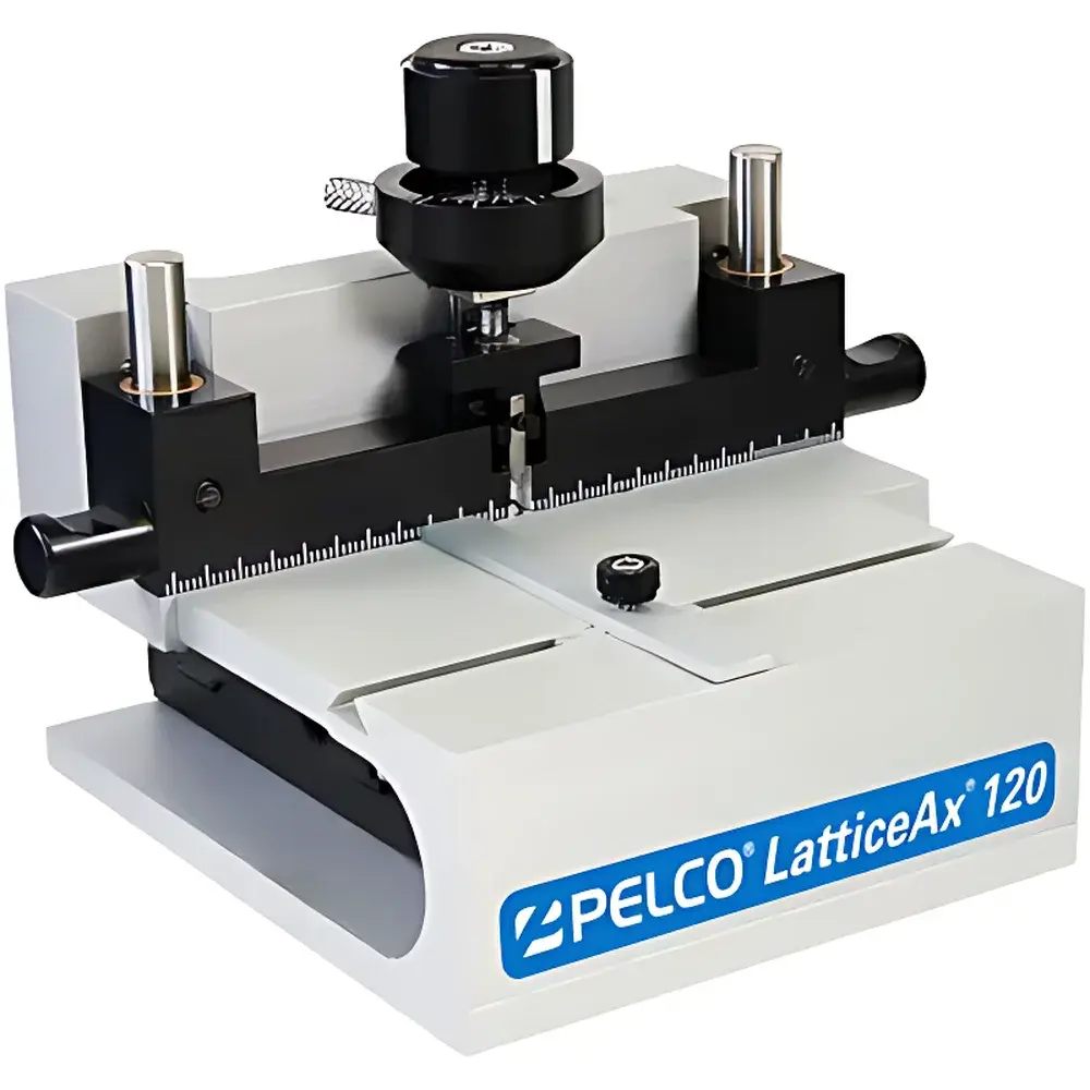
PELCO LatticeAx 120 Manual Wafer Cleaving System
| Brand | Ted Pella |
|---|---|
| Origin | USA |
| Manufacturer Type | Authorized Distributor |
| Origin Category | Imported |
| Model | LatticeAx 120 |
| Maximum Linear Scribing Speed | 100 mm/min |
| Application Scope | Semiconductor Wafers, Compound Semiconductors, Optical Substrates |
Overview
The PELCO® LatticeAx® 120 is a precision-engineered manual wafer cleaving system designed for controlled, crystallographic fracture of brittle semiconductor and optical substrates. Unlike conventional dicing saws that rely on abrasive mechanical cutting or laser ablation, the LatticeAx 120 utilizes lattice-matched cleavage — a non-destructive, stress-induced fracture method aligned with crystalline planes. It operates by first generating a sub-millimeter, ~10 µm wide micro-indentation using a diamond-tipped stylus under vacuum fixation, then applying calibrated three-point bending force to initiate controlled cleavage along low-energy crystallographic planes (e.g., {111} in Si, {110} in GaAs). This technique preserves native microstructure, eliminates kerf loss, avoids thermal damage or recast layers, and yields atomically smooth, mirror-finish cross-sections ideal for high-resolution SEM, TEM lamella pre-thinning, and photonics interface analysis.
Key Features
- Vacuum-mounted sample stage with adjustable tilt and rotation for precise orientation relative to crystal axes
- Integrated linear translation platform with micrometer-driven positioning (±1 µm repeatability) for accurate indentation placement
- Premounted industrial-grade diamond indenter (tip radius: 5–10 µm, Vickers hardness >80 GPa)
- Three-point bending mechanism with calibrated force application (0.5–5 N range), enabling reproducible cleavage initiation without overshoot
- Compact benchtop footprint (305 × 254 × 203 mm) compatible with glovebox, cleanroom Class 1000, and FIB/SEM preparation labs
- No consumables required beyond standard vacuum pump oil; no coolant, slurry, or blade replacement needed
Sample Compatibility & Compliance
The LatticeAx 120 supports cleavage of single-crystal wafers up to 150 mm diameter and thicknesses from 100 µm to 1.2 mm. Verified compatibility includes silicon (Si), gallium arsenide (GaAs), indium phosphide (InP), sapphire (Al₂O₃), fused silica, BK7 glass, and lithium niobate (LiNbO₃). Amorphous or polycrystalline substrates may be cleaved with reduced edge quality but remain viable for macro-scale cross-sectioning. The system complies with ISO 14644-1 Class 5 cleanroom operational guidelines when used with HEPA-filtered vacuum lines. All mechanical components meet RoHS 2011/65/EU directives, and vacuum pump operation adheres to CE 2014/30/EU EMC standards.
Software & Data Management
The LatticeAx 120 is fully manual and does not incorporate embedded firmware or digital control interfaces. However, its mechanical repeatability supports integration into GLP/GMP-compliant workflows: indentation position, applied load, and cleavage direction are documented manually per SOP. Users routinely log parameters in electronic lab notebooks (ELN) compliant with 21 CFR Part 11 requirements when paired with validated documentation systems (e.g., LabArchives, Benchling). Optional accessories include a calibrated digital force gauge (0.01 N resolution) and an optical alignment microscope (10×–50×) for traceable setup verification — both supporting audit-ready calibration records per ISO/IEC 17025.
Applications
- Pre-FIB site-specific cross-sectioning for TEM sample preparation — eliminating ion-beam damage to regions of interest
- Generation of vertical, mirror-finish facets for photonic crystal cavity characterization and waveguide end-face inspection
- Rapid prototyping of diced test structures on non-standard substrates (e.g., thin-film SOI, flexible Si-on-polymer)
- Cross-sectional metrology of epitaxial layer stacks (e.g., AlGaN/GaN HEMT heterostructures) without interfacial delamination
- Preparation of standardized cross-sections for SEM-EDS line scans across device junctions (e.g., p-n diodes, MOS gate stacks)
- Low-damage cleavage of fragile optoelectronic wafers prior to bonding or packaging
FAQ
Does the LatticeAx 120 require electrical power?
No — it is entirely manual and mechanically operated. Only the optional vacuum pump requires AC power (100–240 V, 50/60 Hz).
Can it cleave wafers with patterned topography or metal layers?
Yes, provided the underlying substrate remains crystalline and unfractured; surface metallization may influence crack propagation but does not prevent cleavage.
What is the typical surface roughness (Ra) of cleaved edges?
For oriented Si(100) and GaAs(110), Ra values range from 0.3–0.8 nm as measured by AFM, comparable to cleaved reference standards per ASTM F1725.
Is operator training required for reproducible results?
Yes — consistent cleavage quality depends on crystal orientation alignment and controlled loading rate; Ted Pella provides a certified 4-hour hands-on training module covering ASTM F2749 methodology.
How is maintenance performed?
Annual vacuum pump oil change and stylus tip inspection (via SEM imaging) are recommended; no recalibration is required due to all-mechanical design.


