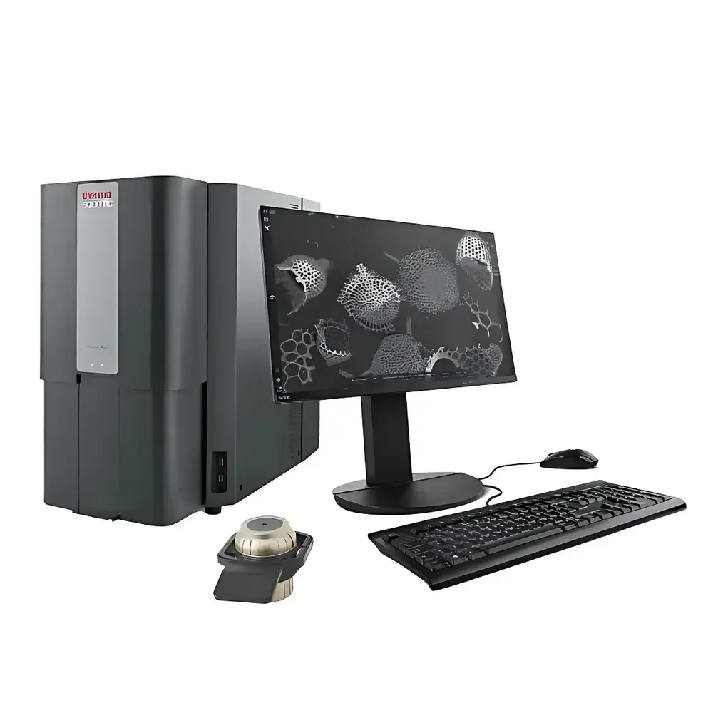
Phenom Pure Desktop Scanning Electron Microscope
| Brand | Phenom |
|---|---|
| Origin | Netherlands |
| Manufacturer | Phenom-World B.V. |
| Type | Desktop SEM |
| Model | Pure |
| Electron Source | Cerium Hexaboride (CeB6) |
| Secondary Electron Resolution | 10 nm |
| Maximum Magnification | 175,000× |
| Accelerating Voltages | 5 kV and 10 kV |
| Backscattered Electron Resolution | 10 nm |
| Vacuum Pump-down Time | <15 s |
| Filament Lifetime | ~1,500 hours |
| Operating Environment | Standard laboratory or office floor (anti-vibration design) |
Overview
The Phenom Pure Desktop Scanning Electron Microscope is a sixth-generation benchtop SEM engineered for high-resolution imaging of sub-micron surface topography and compositional contrast without the infrastructure demands of conventional floor-standing systems. Utilizing a high-brightness cerium hexaboride (CeB6) thermionic electron source, the Pure delivers stable beam current and superior signal-to-noise ratio at accelerating voltages of 5 kV and 10 kV—optimally balancing surface detail, reduced charging artifacts on insulating samples, and material interaction depth. Its 10 nm secondary electron (SE) and backscattered electron (BSE) resolution enables reliable visualization of nanoscale features in metals, ceramics, polymers, geological specimens, biological tissues (with minimal or no conductive coating), and advanced materials such as battery electrodes or semiconductor packaging. Designed for integration into routine QA/QC workflows, academic teaching labs, and R&D screening environments, the Pure operates independently of dedicated EM rooms, requiring only standard AC power and ambient lab conditions.
Key Features
- High-stability CeB6 electron source with typical operational lifetime exceeding 1,500 hours—reducing maintenance frequency and cost of ownership.
- Automated vacuum system achieving full operational vacuum in under 15 seconds, enabling rapid sample turnover and high-throughput inspection.
- Integrated high-sensitivity quadrant backscattered electron (BSE) detector for simultaneous topographic and atomic-number contrast imaging.
- No-coating operation capability for non-conductive samples (e.g., plastics, ceramics, uncoated biological sections), minimizing preparation time and preserving native morphology.
- Robust anti-vibration mechanical architecture, allowing stable operation on standard laboratory benches or office-grade flooring without external isolation tables.
- Intuitive one-button workflow interface with real-time image acquisition, auto-focus, auto-stigmation, and stage navigation—designed for users with minimal SEM training.
Sample Compatibility & Compliance
The Phenom Pure accommodates samples up to 100 mm in diameter and 40 mm in height, supporting diverse specimen geometries including bulk solids, powders, filters, wafers, and mounted cross-sections. Its low-kV imaging mode (5 kV) significantly mitigates surface charging on insulators, eliminating the need for sputter coating in many applications—a critical advantage for failure analysis, forensic examination, and educational use. The instrument complies with IEC 61000-6-3 (EMC emission standards) and IEC 61000-6-2 (immunity), and its software architecture supports audit-ready data handling aligned with GLP and GMP principles. While not certified for regulated pharmaceutical manufacturing per FDA 21 CFR Part 11 out-of-the-box, raw image metadata—including timestamp, HV, WD, magnification, and detector settings—is embedded in TIFF/SEM format files for traceable documentation.
Software & Data Management
Acquisition and analysis are performed via Phenom Desktop Software, a Windows-based platform featuring real-time image stitching, particle analysis (size, shape, count), EDS integration readiness (via optional add-on), and measurement annotation tools calibrated to stage encoder feedback. All images retain embedded EXIF-style metadata, facilitating reproducibility and regulatory documentation. Data export supports TIFF, PNG, JPEG, and CSV formats; batch processing scripts can be configured for standardized reporting across multi-user facilities. The software architecture permits role-based user accounts and optional password-protected configuration lockdown—supporting controlled access in shared lab environments.
Applications
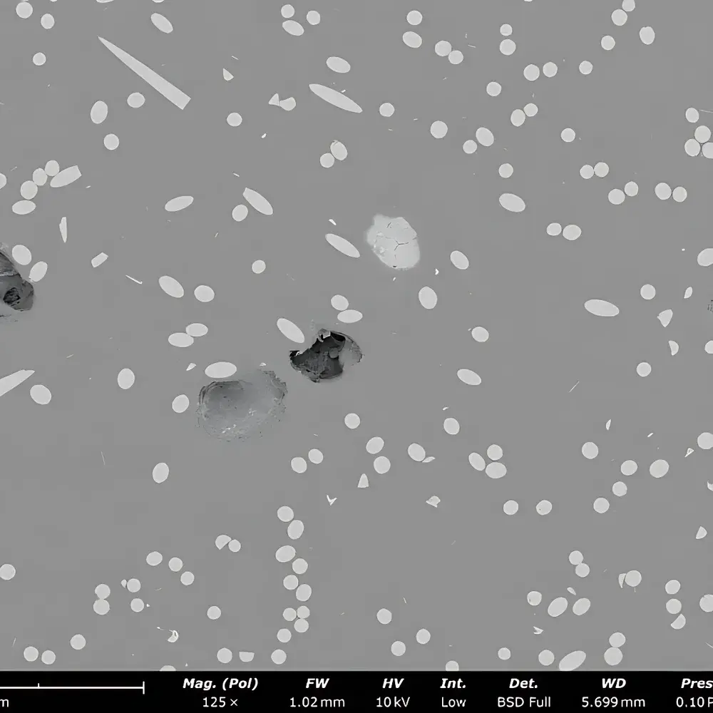
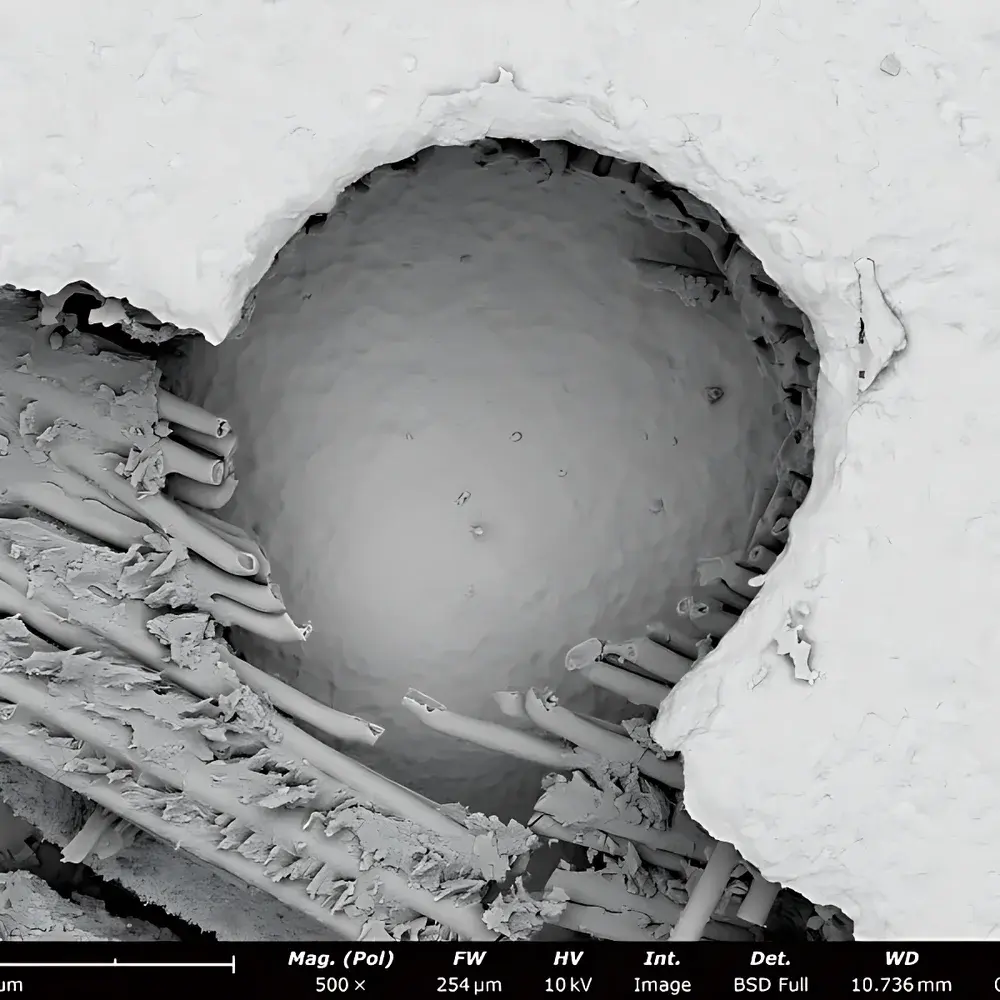
- Materials science: Grain boundary analysis, fracture surface characterization, porosity quantification in catalysts and composites.
- Electronics: Solder joint inspection, PCB trace integrity assessment, contamination identification on IC packages.
- Life sciences: Uncoated pollen grain morphology, diatom frustule imaging, tissue scaffold microstructure evaluation.
- Geosciences: Mineral phase discrimination via BSE contrast, pore network analysis in shale cores.
- Quality control: Rapid verification of coating uniformity, fiber diameter distribution in nonwovens, defect mapping in additive-manufactured parts.
- Education: Hands-on SEM instruction at undergraduate and graduate levels, supporting curriculum-aligned experiments in microscopy, metallurgy, and nanotechnology.
FAQ
Does the Phenom Pure require liquid nitrogen or external water cooling?
No—the CeB6 source operates with air cooling only, eliminating cryogenic dependencies and service overhead.
Can the system be upgraded to include energy-dispersive X-ray spectroscopy (EDS)?
Yes—Phenom offers an EDS-ready configuration with compatible port geometry and software hooks; third-party detectors may be integrated subject to mechanical and electrical compatibility validation.
What is the recommended maintenance schedule?
Routine cleaning of the viewport and chamber interior is advised every 2–3 months; filament replacement is typically required every 18–24 months under normal usage (≈1,500 h). No pump oil changes are needed—the turbomolecular pump is sealed and maintenance-free.
Is remote operation supported?
Yes—via secure RDP or VNC protocols over local networks; full control, image acquisition, and measurement functions remain available remotely.
How does the Pure compare to field-emission SEMs (FE-SEM) in resolution performance?
While FE-SEMs achieve sub-nanometer resolution under ultra-high vacuum and cryo-conditions, the Pure provides robust 10 nm resolution under high-throughput, low-cost, and user-accessible conditions—making it optimal for screening, teaching, and routine industrial inspection where ultimate resolution is secondary to speed, simplicity, and total cost of ownership.


