Photonic Science OEM Camera Solutions – Custom-Designed Scientific Imaging Systems
| Origin | UK |
|---|---|
| Manufacturer Type | Authorized Distributor |
| Origin Category | Imported |
| Model | OEM Camera Platform |
| Price Range | USD 42,000 – 70,000 |
Overview
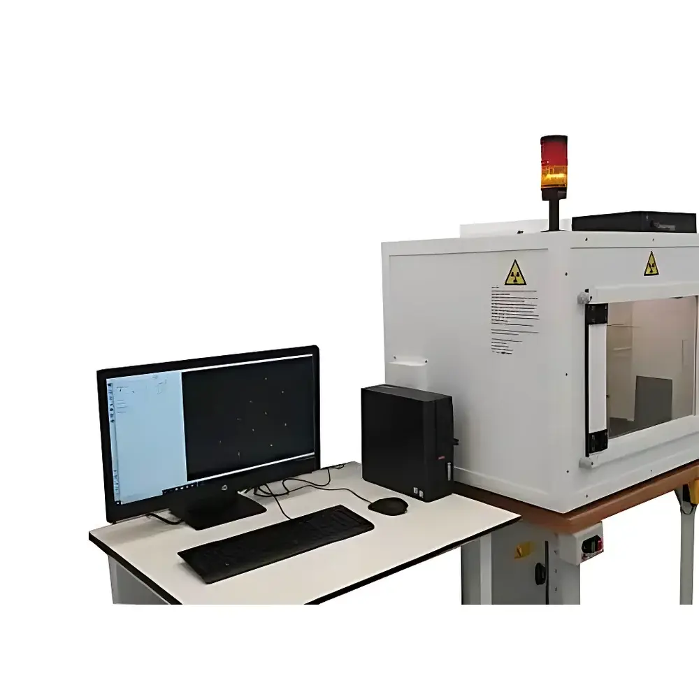
Photonic Science OEM Camera Solutions represent a comprehensive, engineering-led platform for integrating high-performance scientific imaging subsystems into third-party instruments and industrial systems. Designed and manufactured in the United Kingdom, these solutions are built upon Photonic Science’s core competency in low-noise, high-fidelity photon detection across spectral bands spanning ultraviolet (UV), visible (VIS), near-infrared (NIR), short-wave infrared (SWIR: up to 2.2 µm), extreme ultraviolet (EUV), soft and hard X-ray, and neutron radiation. The platform leverages proven sensor technologies—including back-illuminated sCMOS, EMCCD, CCD, InGaAs-based SWIR, and intensified ICCD—and integrates them with application-specific electronics, thermal management, mechanical packaging, and firmware. Unlike off-the-shelf cameras, these OEM systems are architected from first principles to meet defined optical, electrical, thermal, and mechanical interfaces—ensuring seamless integration into end-user equipment used in synchrotron beamlines, semiconductor metrology tools, defense-grade surveillance platforms, medical imaging devices, and industrial non-destructive testing (NDT) systems.
Key Features
- Multi-spectral sensor support: UV-VIS-NIR sCMOS (e.g., Gpixel 4k×4k, BAE/Fairchild HD sCMOS), SWIR InGaAs (640×512 & 320×256 formats, 15 µm & 25 µm pixel pitch), ICCD/ICCD-Neutron, EUV/X-ray direct-detection and scintillator-coupled configurations
- Thermal architecture options: Compact deep-cooling modules (down to −45 °C) for ultra-low dark current; air- or liquid-cooled variants; thermoelectrically stabilized heads with active feedback control
- Modular mechanical design: Fully customizable housing—ranging from bare sensor boards to hermetically sealed, MIL-STD-810G-compliant enclosures—with user-defined mounting flanges, I/O port locations, and SWaP (Size, Weight, and Power) optimization
- Interface flexibility: GenICam-compliant firmware stack; Camera Link (Base/Medium/Full), CoaXPress, or custom digital interface; remote control via Ethernet or RS-422 with programmable trigger and synchronization logic
- Firmware customization: Field-upgradable FPGA-based processing pipelines—including real-time binning, region-of-interest (ROI) readout, on-chip offset/gain correction, and user-defined LUTs—developed per OEM specification
- Environmental qualification: Full environmental testing including thermal cycling (−40 °C to +70 °C), mechanical shock (50 g, 11 ms), and random vibration (10–2000 Hz, 0.04 g²/Hz)
Sample Compatibility & Compliance
The OEM Camera Platform supports diverse sample interaction modalities—including transmission, reflection, fluorescence, phosphorescence, Laue diffraction, radioluminescence, and time-resolved luminescence—enabling integration into analytical instruments such as micro-CT scanners, PL (photoluminescence) mapping stations, X-ray topography systems, and neutron radiography setups. All systems comply with ISO 9001:2015 quality management requirements. Where applicable, designs adhere to electromagnetic compatibility (EMC) standards per EN 61326-1, and mechanical robustness aligns with MIL-STD-810H for defense applications. Firmware and data handling protocols can be configured to support audit trails and electronic signatures in accordance with FDA 21 CFR Part 11 for regulated environments.
Software & Data Management
OEM customers receive full access to Photonic Science’s Software Development Kit (SDK), which includes C/C++, Python, and MATLAB APIs compliant with GenICam SFNC v2.4. The SDK supports synchronized multi-camera acquisition, hardware-triggered burst modes, and metadata embedding (timestamp, temperature, exposure, gain). For turnkey system integrators, Photonic Science provides optional embedded software modules—including Laue orientation analysis engines, X-ray tomographic reconstruction kernels, and SWIR spectral calibration utilities—that may be licensed under OEM terms. All firmware updates are digitally signed and delivered via secure repository access, ensuring traceability and version control throughout product lifecycle.
Applications
- Synchrotron and FEL beamline diagnostics: Time-resolved X-ray imaging, pump-probe experiments, single-shot diffraction
- Industrial NDT: Real-time micro-CT inspection of turbine blades, battery electrode porosity analysis, weld integrity assessment
- Defense & aerospace: SWIR surveillance under low-light conditions, laser spot tracking, missile seeker head development
- Life sciences: High-speed calcium imaging, super-resolution PALM/STORM, time-gated FLIM
- Materials science: In-situ Laue crystallography, strain mapping, phase transformation monitoring under thermal/mechanical load
- Semiconductor metrology: EUV mask inspection, wafer defect review using backside illumination
FAQ
Can Photonic Science provide camera systems compliant with ITAR or EAR export control regulations?
Yes—design documentation, firmware binaries, and hardware configurations can be structured to meet EAR99 or specific ECCN classifications, with export licenses coordinated through Photonic Science’s UK-based compliance office.
Is it possible to integrate custom optical components—such as fiber-optic tapers or microchannel plates—into the OEM camera head?
Absolutely. Photonic Science routinely couples sensors to fiber-optic faceplates, MCP stacks, and scintillators (e.g., Gd₂O₂S:Tb, CsI:Tl, LYSO) via vacuum deposition or optical bonding, with performance validation included in the qualification protocol.
What level of firmware customization is supported for real-time image processing?
FPGA-based logic can implement user-defined algorithms—including centroid calculation, edge detection, histogram equalization, and pixel-level gain correction—with latency under 10 µs for critical timing applications.
Do you offer long-term supply assurance and obsolescence management for OEM programs?
Yes—Photonic Science maintains component lifetime roadmaps, dual-sourcing strategies for key semiconductors, and formal last-time-buy planning aligned with customer production schedules.
Are mechanical drawings and thermal simulation reports available during the design phase?
Full CAD models (STEP, IGES), thermal FEA reports, and tolerance stack-up analyses are delivered at Design Review Milestone 3 (DR3) as part of the engineering collaboration process.


