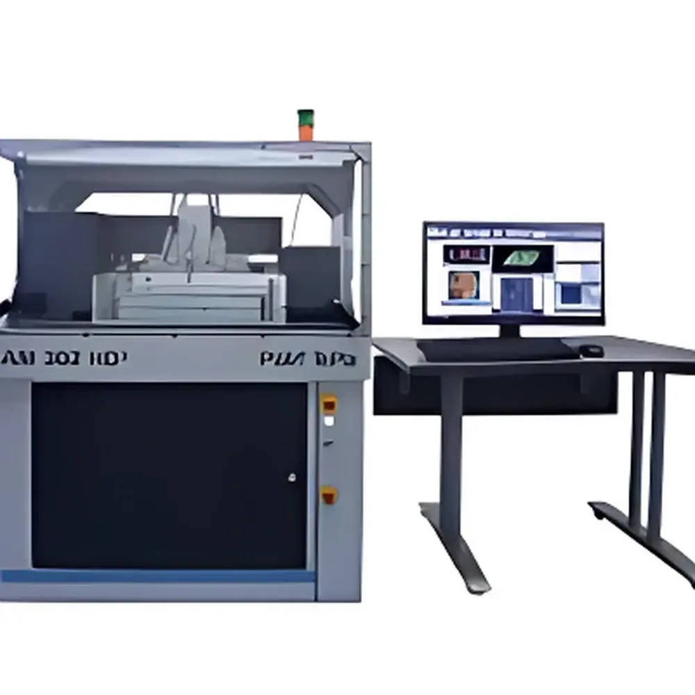
PVA TePla SAM Premium Ultrasonic Scanning Microscope
| Brand | PVA TePla |
|---|---|
| Origin | USA |
| Manufacturer Type | Authorized Distributor |
| Import Status | Imported |
| Model | SAM Premium |
| Pricing | Available Upon Request |
Overview
The PVA TePla SAM Premium Ultrasonic Scanning Microscope is a high-precision, non-destructive evaluation (NDE) platform engineered for critical defect detection and internal structural characterization in semiconductor wafers, packaged ICs, power modules, MEMS devices, and advanced electronic assemblies. It operates on the principle of pulse-echo acoustic microscopy—transmitting high-frequency ultrasonic waves (5–400 MHz, extendable to 1000 MHz via optional HiSA-compatible transducers) into a sample immersed in coupling fluid (typically deionized water), then detecting time-resolved echoes reflected from acoustic impedance mismatches at material interfaces or subsurface discontinuities. Unlike optical or electron-based techniques, ultrasonic scanning provides depth-resolved, three-dimensional volumetric imaging without sample preparation, ionizing radiation, or vacuum requirements—making it indispensable for inline process monitoring, failure analysis (FA), and reliability qualification in cleanroom environments.
Key Features
- Hybrid multimodal architecture integrating full-featured inverted or epi-reflective optical microscopy with synchronized acoustic scanning—enabling direct correlation between surface morphology and subsurface anomalies.
- Wide frequency spectrum support: standard transducer options from 5 MHz to 400 MHz; optional ultra-high-frequency (UHF) transducers up to 1000 MHz for sub-micron axial resolution in thin-film and TSV (through-silicon via) inspection.
- Intelligent auto-focus per transducer: real-time dynamic focusing compensates for surface topography variations during scanning, ensuring consistent signal-to-noise ratio across curved or warped samples (e.g., 300 mm wafers with bow ≤ 50 µm).
- Modular scanning stage with configurable X-Y travel: selectable ranges from 250 µm × 250 µm (for high-resolution die-level analysis) up to 502 mm × 502 mm (for full-panel or substrate-level inspection).
- HiSA (High-Speed Scanning Axis) technology: enables continuous dynamic focusing while maintaining scan speeds up to 200 mm/s—critical for throughput-sensitive applications such as wafer-level burn-in screening or post-dicing delamination mapping.
- Dynamic Through-Scan (DTS) mode: supports frequency-agile scanning between 25 MHz and 100 MHz within a single acquisition, optimizing contrast for layered structures (e.g., bond interface vs. bulk silicon).
Sample Compatibility & Compliance
The SAM Premium accommodates rigid and semi-rigid substrates including silicon, GaAs, SiC, glass, ceramic packages (QFN, BGA, WLP), and flexible printed circuits (FPCs). Samples are mounted on vacuum chucks or custom fixtures compatible with SEM-style stage interfaces. The system complies with ISO 17025 calibration traceability requirements for measurement uncertainty reporting and supports audit-ready documentation per GLP/GMP and IATF 16949 frameworks. All acoustic data acquisition protocols adhere to ASTM E1783 (Standard Practice for Acoustic Microscopy of Electronic Components) and JEDEC JESD22-A108 (Temperature Cycling) for reliability test correlation.
Software & Data Management
Controlled by PVA TePla’s proprietary SAM-Studio software suite, the platform delivers intuitive workflow-driven operation—from automated recipe-based scanning to multi-parameter image fusion (A-scan, B-scan, C-scan, S-scan, and 3D volume rendering). Raw RF echo data is stored in HDF5 format with embedded metadata (transducer ID, gain, PRF, gate settings, temperature, operator ID), ensuring full traceability. Software features FDA 21 CFR Part 11-compliant user access control, electronic signatures, and immutable audit trails. Export options include TIFF, PNG, CSV, and DICOM-SR for integration with FA lab LIMS or enterprise MES systems.
Applications
- Delamination detection at die-attach, mold compound–leadframe, and wafer-level underfill interfaces.
- Void and porosity quantification in solder bumps, copper pillars, and electroplated TSVs.
- Crack propagation analysis in low-k dielectrics and passivation layers after thermal stress testing.
- Non-contact thickness measurement of transparent thin films (e.g., SiO₂, SiNₓ) on silicon substrates using time-of-flight calibration.
- Qualification of advanced packaging technologies: Fan-Out Wafer-Level Packaging (FOWLP), 2.5D/3D IC stacking, and heterogeneous integration assemblies.
FAQ
What is the minimum detectable defect size using the SAM Premium at 200 MHz?
Typical lateral resolution is ~7–10 µm; axial resolution is ~2–3 µm—dependent on transducer focal length, coupling medium, and sample acoustic properties.
Can the system perform automated pass/fail classification based on acoustic thresholds?
Yes—SAM-Studio supports rule-based defect classification with customizable ROI masking, intensity thresholding, and area/volume filtering, exportable as CSV reports compliant with IPC-A-610 and AEC-Q200 standards.
Is the system compatible with front-end semiconductor fab environments?
Fully compatible: Class 100 cleanroom-rated enclosure, ESD-safe design (IEC 61340-5-1), and SECS/GEM interface option for factory automation integration.
Does PVA TePla provide application support for failure analysis workflows?
Yes—dedicated FA engineering team offers remote diagnostics, method development, and on-site training aligned with JEDEC, IPC, and SEMI standards.


