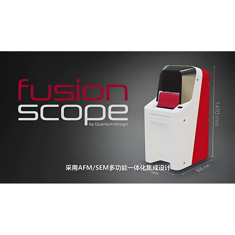
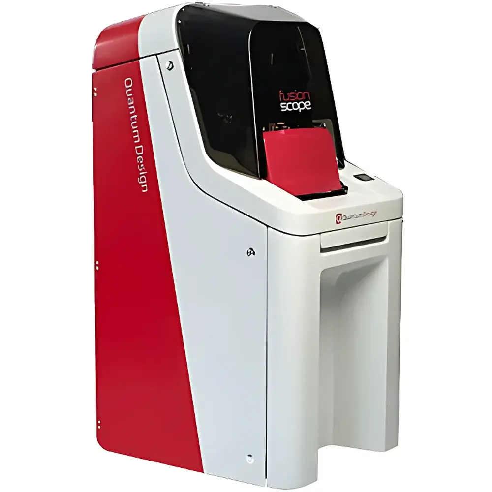
Quantum Design FusionScope AFM-SEM Integrated In-Situ Microscope
| Brand | Quantum Design |
|---|---|
| Origin | USA |
| Manufacturer Type | Original Equipment Manufacturer (OEM) |
| Product Category | Imported Instrument |
| Model | FusionScope |
| Instrument Type | Materials-Focused Hybrid AFM/SEM System |
| Positional Detection Noise | <50 pm @ 1 kHz |
| Maximum Sample Diameter | ≤20 mm |
| Maximum Sample Height | ≤20 mm |
| Sample Stage Travel Range | XY: 22 × 22 µm (closed-loop), Z: 15 µm |
Overview
The Quantum Design FusionScope is a purpose-engineered, in-situ hybrid microscope that unifies scanning electron microscopy (SEM) and atomic force microscopy (AFM) within a single vacuum-compatible platform. Unlike conventional correlative workflows requiring physical sample transfer between separate instruments—introducing positional uncertainty, contamination risk, and time loss—the FusionScope establishes a true shared coordinate system. Its core innovation lies in the synchronized operation of a thermally assisted field-emission SEM column and a high-stability, self-sensing AFM module, both operating under ultra-high vacuum (UHV)-compatible conditions (1–10 µTorr). This architecture enables simultaneous or sequential acquisition of topographic, compositional, mechanical, electrical, magnetic, and chemical data from identical nanoscale regions—without repositioning, realignment, or environmental exposure. The system is engineered for precision metrology in advanced materials research, semiconductor process development, nanomechanical characterization, and life science applications where spatial fidelity, environmental control, and multimodal correlation are non-negotiable.
Key Features
- In-situ AFM-SEM coordinate registration: Real-time SEM navigation guides AFM probe placement with sub-100 nm accuracy; no sample relocation required.
- Self-sensing piezoresistive cantilevers: Eliminates optical alignment complexity; delivers low-noise (<50 pm @ 1 kHz), high-bandwidth deflection signals directly via integrated strain gauges.
- Integrated EDS capability: Energy-dispersive X-ray spectroscopy add-on enables elemental mapping concurrent with topographic and property imaging.
- 80° sample tilt & dual-axis rotation: Enables sidewall imaging, cross-sectional profiling, and oblique-angle nanomechanical testing under direct SEM observation.
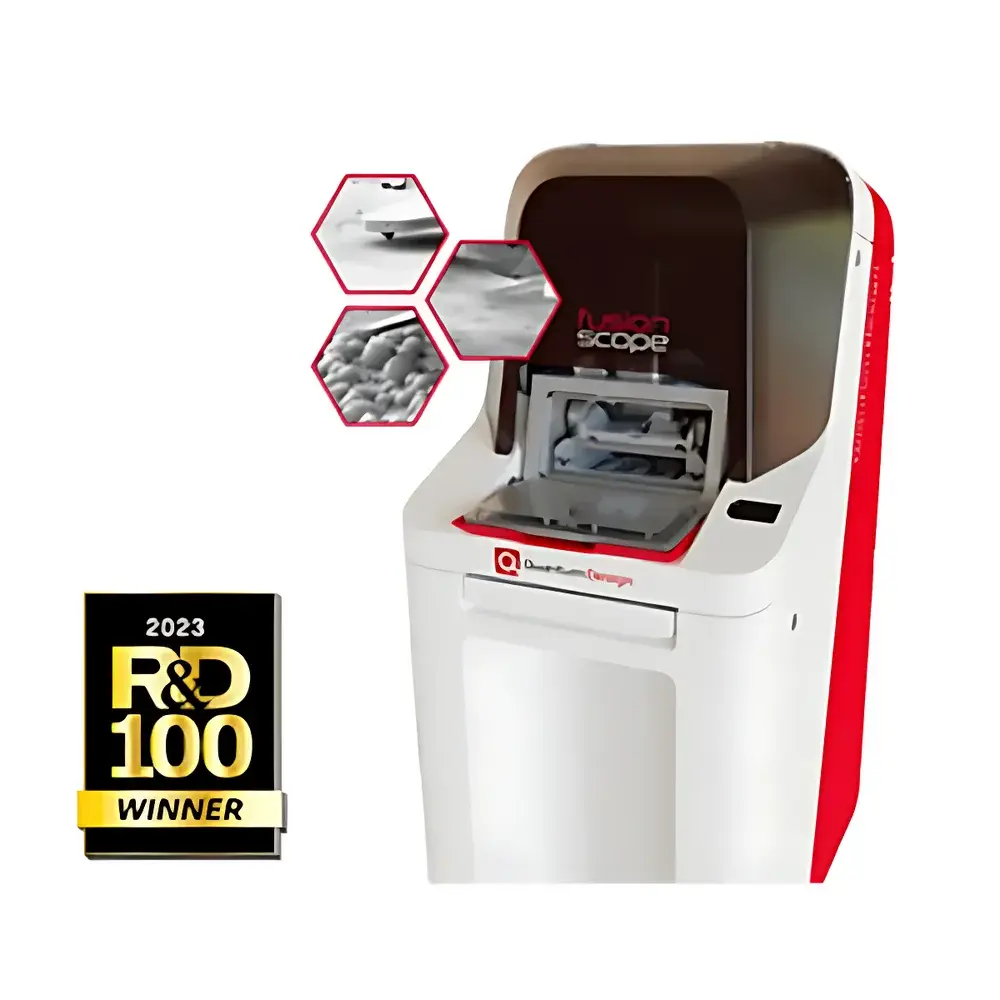
- Real-time profile imaging mode: Visualizes cantilever tip position relative to sample surface during approach—critical for fragile, suspended, or high-aspect-ratio nanostructures (e.g., graphene membranes, nanowires).
- Modular AFM modes: Supports contact, dynamic (tapping), FIRE (Finite Impulse Response Excitation), conductive AFM (C-AFM), magnetic force microscopy (MFM), and electrostatic force microscopy (EFM) via interchangeable functional probes.
- Automated workflow architecture: Task-based GUI with guided wizards reduces setup time; supports user-defined interface layouts, experiment logging, and annotation tagging.
Sample Compatibility & Compliance
The FusionScope accommodates samples up to 20 mm in diameter and 20 mm in height (500 g max weight), with automated stage alignment and vacuum lock mechanisms ensuring repeatable positioning. Its chamber design supports ambient-to-UHV transitions (<5 min pump-down), making it suitable for air-sensitive materials—including 2D crystals (graphene, MoS₂), organic semiconductors, biological specimens (dehydrated or cryo-stabilized), and catalytic nanoparticles. All hardware and software comply with ISO/IEC 17025 traceability requirements for measurement systems. Data acquisition logs meet GLP/GMP audit-trail standards per FDA 21 CFR Part 11, including electronic signatures, version-controlled parameter sets, and immutable experiment metadata export. EDS spectral quantification adheres to ASTM E1508 and ISO 16593 protocols.
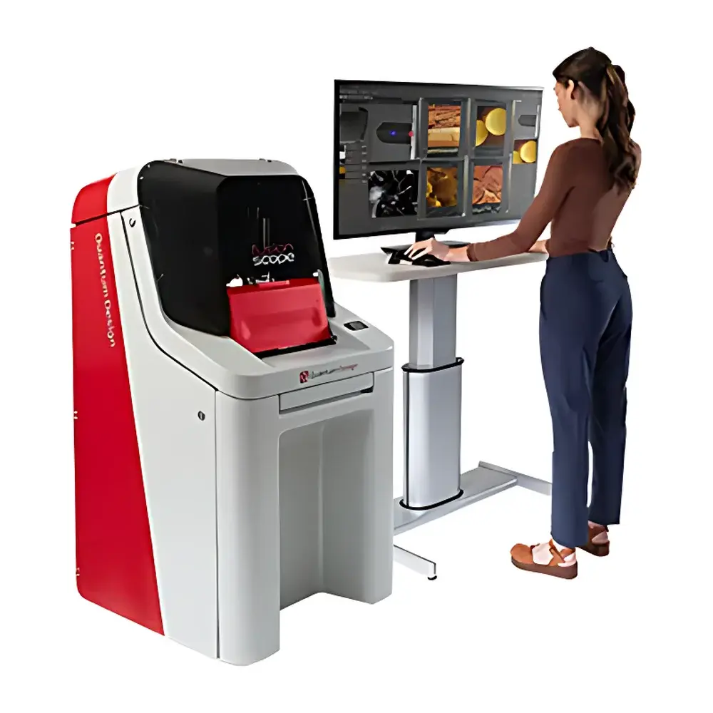
Software & Data Management
FusionScope Control Software provides unified operation of both SEM and AFM subsystems through a dual-mode interface: Standard Mode for rapid acquisition and Advanced Mode for scripting, multi-channel synchronization, and custom feedback loop configuration. Each experiment is saved as a self-contained .fusionexp file containing raw sensor streams, metadata (voltage, current, dwell time, gain settings), and calibrated coordinate transforms. Native integration with Gwyddion enables batch processing of AFM topography, phase, and force-volume datasets. SEM-EDS spectra are exported in standard .emsa format for quantitative analysis in Thermo Fisher Avizo or Oxford Instruments AZtec. All data paths support network-mounted storage and DICOM-compliant metadata embedding for institutional LIMS interoperability.
Applications
- Semiconductor metrology: Sub-5 nm transistor gate profiling, interconnect roughness quantification, and localized conductivity mapping on full-die wafers without sample relocation.
- Nanomechanics: In-situ nanoindentation with real-time load-displacement curve capture; spatially resolved modulus mapping across grain boundaries in polycrystalline alloys.
- 2D material characterization: Simultaneous SEM visualization and AFM-based strain mapping of suspended graphene; controlled mechanical deformation studies under electron beam observation.
- Magnetic and ferroelectric domain analysis: Correlated MFM/EFM phase imaging with SEM crystallographic contrast—e.g., domain wall pinning at grain boundaries in Co/Pt multilayers or BaTiO₃ ceramics.
- Life science structural biology: High-resolution 3D morphology of bone lacunae, collagen fibril periodicity, and diatom frustule nanoarchitecture—all under controlled vacuum conditions preserving native topology.
FAQ
How does the FusionScope maintain spatial correlation between AFM and SEM images?
It employs a monolithic, kinematically aligned stage with integrated encoders and laser interferometer feedback, referenced to a common fiducial grid etched into the sample holder—enabling <100 nm positional repeatability across modalities.
Can the system operate in variable pressure or environmental modes?
No—the FusionScope is optimized for high-vacuum operation (1–10 µTorr) to ensure stable AFM performance and minimize electron scattering; it is not configured for ESEM or gas injection environments.
Is third-party probe compatibility supported?
Yes—standard 125 µm × 125 µm × 4 µm silicon cantilevers with piezoresistive readout are compatible; however, optimal noise performance requires Quantum Design–certified self-sensing probes fabricated via FEBID.
What level of training is required to operate the system independently?
A two-day on-site installation and operation course covers basic alignment, mode switching, and data export; advanced techniques (e.g., force spectroscopy, EFM bias ramping) are covered in optional application-specific workshops.
Does the system support automated feature recognition and region-of-interest targeting?
Yes—integrated machine vision algorithms identify edges, particles, or defects in SEM preview scans and auto-generate AFM scan frames with sub-micron centering accuracy.


