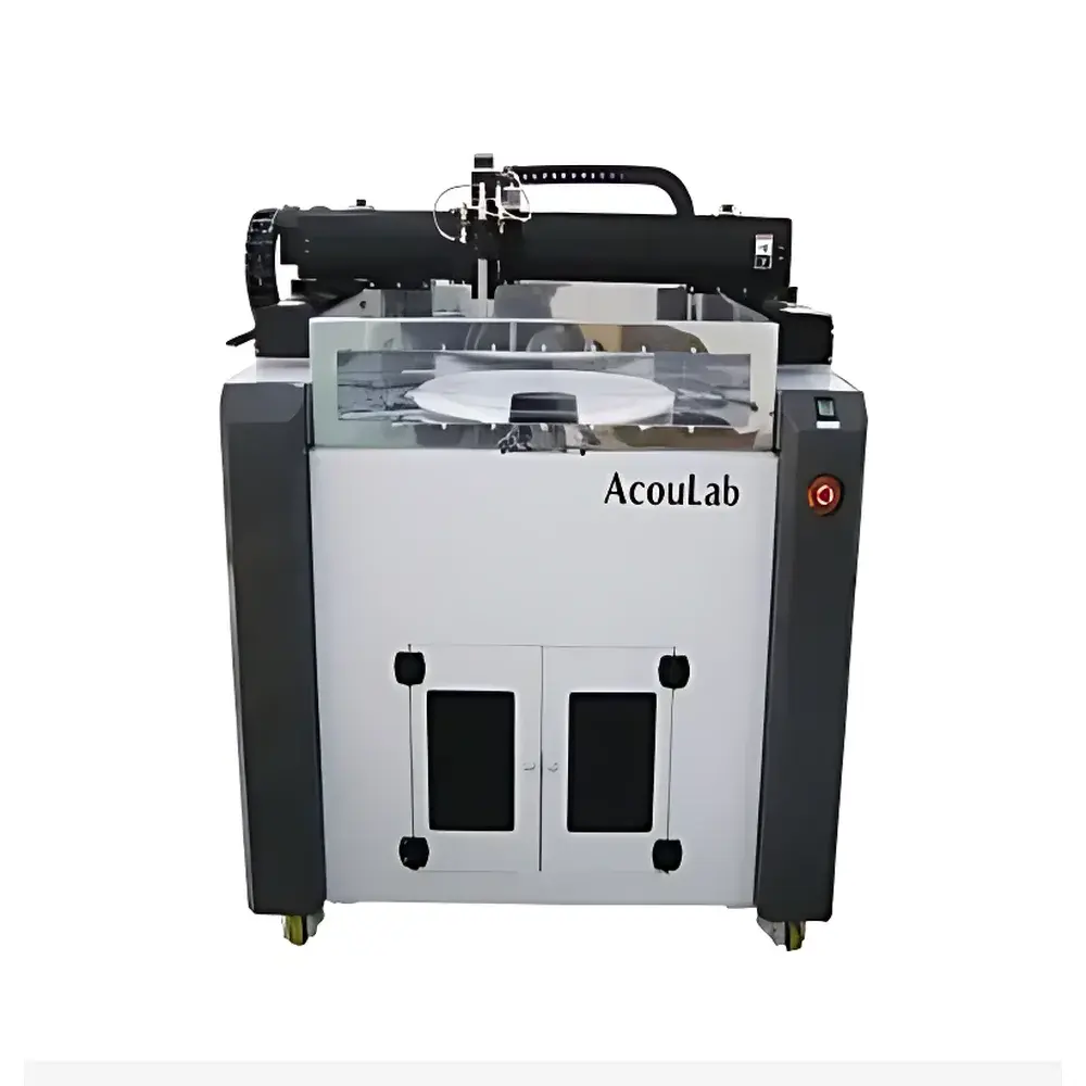
SAM-SPICA Scanning Acoustic Microscope by Acoulab
| Brand | Acoulab |
|---|---|
| Origin | South Korea |
| Model | SAM-SPICA |
| Instrument Type | Digital Scanning Acoustic Microscope |
| Transducer Frequency Range | 1–500 MHz |
| A/D Sampling Rate | 500 MHz |
| Signal Bandwidth | 1 GHz |
| XY Scan Speed | 1000 mm/s |
| XY Repeatability | ±0.5 µm |
| Scan Modes | A-scan, B-scan, C-scan, X-scan (multi-layer C-scan) |
| Sample Handling | Motorized tilt/rotation/translation stage with liquid coupling tank compatibility |
Overview
The SAM-SPICA Scanning Acoustic Microscope (SAM) is a high-resolution, non-destructive evaluation (NDE) system engineered for subsurface defect characterization in advanced materials and microelectronic packages. Operating on the principle of pulse-echo ultrasonic imaging, it utilizes high-frequency acoustic waves (1–500 MHz) to interrogate internal structures with micron-level spatial resolution. Unlike optical or X-ray techniques, SAM leverages acoustic impedance mismatches at material interfaces to generate contrast—enabling precise detection of delaminations, voids, cracks, inclusions, and interfacial anomalies without sample preparation or radiation exposure. The system employs immersion coupling via deionized water or specialized acoustic fluids, ensuring consistent wave transmission and minimal signal attenuation. Its modular architecture supports integration into failure analysis (FA) laboratories, semiconductor packaging QA/QC workflows, and metal component reliability testing environments compliant with ASTM E1781, ISO 16932, and JEDEC JESD22-A108 standards.
Key Features
- High-frequency transducer capability (1–500 MHz) with broadband 1 GHz analog front-end and 500 MHz digitization, enabling sub-micron axial resolution in dense materials such as copper substrates, silicon dies, and ceramic packages.
- Motorized XYZ stage with integrated tilt (±15°), rotation (360° continuous), and translation axes—designed for multi-angle interrogation of complex geometries including IGBT modules, power capacitors, and forged engine components.
- Dual-axis high-speed linear servo drive system (X/Y), achieving 1000 mm/s scan velocity while maintaining ±0.5 µm positional repeatability—critical for high-throughput C-scan mapping across wafers or large-area metal plates.
- Multi-mode acquisition architecture supporting A-scan (time-domain waveform), B-scan (cross-sectional slice), C-scan (planar amplitude/phase map at defined depth), and X-scan (automated depth-resolved stack generation for 3D reconstruction).
- Low-noise RF signal chain and adaptive gain control ensure high signal-to-noise ratio (SNR) across heterogeneous samples—from aluminum alloy castings to epoxy-molded ICs—minimizing false positives during automated defect classification.
- Modular liquid coupling chamber design allows customization of tank volume, transducer mounting configuration, and temperature-controlled immersion media—supporting both standard water bath and low-volatility fluid options for sensitive optoelectronic assemblies.
Sample Compatibility & Compliance
The SAM-SPICA accommodates a broad spectrum of industrial and semiconductor specimens: metallic components (steel forgings, nonferrous alloys, weld zones, piston assemblies), ceramic substrates, silicon wafers, TSV-packaged devices, molded ICs (QFN, BGA, LGA), copper baseplates, and composite laminates. It meets functional requirements for GLP/GMP-aligned failure analysis labs, with audit-ready data logging, user-access controls, and timestamped metadata per scan session. System output conforms to ASTM E1158 (standard guide for acoustic emission monitoring), ISO 18563-1 (non-destructive testing—ultrasonic testing—characterization of equipment), and supports traceability under FDA 21 CFR Part 11 when deployed with validated software configurations.
Software & Data Management
Acoulab’s proprietary SAMView™ software provides real-time image processing, depth-gated analysis, automatic threshold-based defect segmentation, and quantitative measurement tools (defect area, depth, aspect ratio, volumetric estimation). All raw RF data are stored in HDF5 format with embedded calibration metadata, ensuring full reproducibility. Export options include DICOM-SAM, TIFF stacks, CSV reports, and STL-compatible 3D surface meshes. The platform supports scripting via Python API for integration into automated FA pipelines and statistical process control (SPC) dashboards. Audit trails record operator ID, instrument parameters, calibration timestamps, and modification history—meeting regulatory expectations for analytical instrument qualification (AIQ) and data integrity frameworks.
Applications
- Semiconductor: Detection of die attach voids, mold compound delamination, wire bond lift-off, and TSV fill defects in advanced packaging (2.5D/3D IC, fan-out wafer-level packaging).
- Power Electronics: Inspection of solder joint integrity, copper diffusion barrier failures, and thermal interface layer discontinuities in IGBT modules and SiC power devices.
- Metallic Components: Assessment of hydrogen-induced cracking (HIC), porosity in investment castings, inclusion distribution in rolled steel, and fusion zone integrity in laser-welded automotive joints.
- Advanced Materials: Characterization of interfacial adhesion in metal-ceramic composites, fiber-matrix debonding in CFRP, and microcrack propagation in thermal barrier coatings.
- Research & Development: Quantitative correlation of acoustic attenuation spectra with microstructural evolution during heat treatment, fatigue cycling, or electromigration stress testing.
FAQ
What types of defects can SAM-SPICA detect in semiconductor packages?
It identifies delamination at die-attach, mold compound–leadframe interfaces, voids in underfill or solder bumps, wire bond separations, and cracks in silicon dies or passivation layers.
Is the system suitable for analyzing large-area metal components such as engine blocks or turbine blades?
Yes—the motorized stage supports customizable travel ranges up to 300 × 300 mm, and optional extended Z-axis modules accommodate parts up to 150 mm thick with uniform focus across the field of view.
Can SAM-SPICA perform quantitative 3D reconstruction of subsurface features?
Yes—through synchronized multi-depth C-scan acquisition and post-processing in SAMView™, users generate volumetric renderings with calibrated depth scaling and iso-surface extraction for metrology-grade reporting.
Does the system support compliance with industry-specific validation protocols?
Yes—documentation packages include IQ/OQ/PQ templates aligned with ISO/IEC 17025 and GAMP5 guidelines, along with traceable calibration certificates for transducers and positioning encoders.
How is acoustic coupling maintained during long-duration scans or elevated temperature testing?
The liquid tank includes recirculation filtration, degassing, and optional Peltier-based temperature stabilization (±0.1°C), ensuring stable acoustic impedance and minimizing thermal drift artifacts in time-lapse studies.


