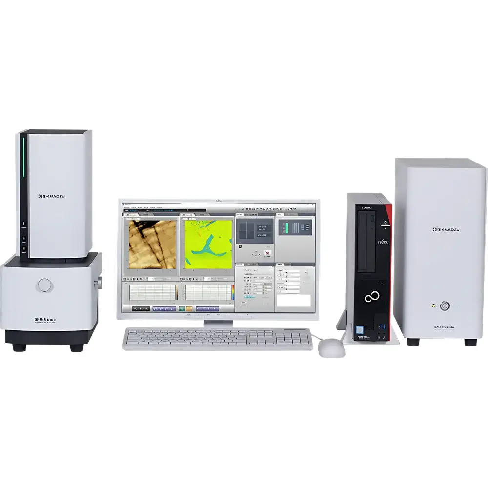
Shimadzu SPM-Nanoa Atomic Force Microscope
| Brand | Shimadzu |
|---|---|
| Origin | Japan |
| Manufacturer | Shimadzu Corporation |
| Instrument Type | Atomic Force Microscope (AFM) |
| Category | Materials AFM |
| Position Detection Noise | < 0.02 nm RMS |
| Sample Dimensions | Ø50 mm × 8 mm max thickness |
| XY Stage Travel Range | 5 mm × 5 mm |
| Imaging Resolution | Up to 8192 × 8192 pixels |
| Automation Features | Auto-alignment ("Link On"), Auto-parameter optimization ("NanoAssist"), Fully automated tip exchange and fast 3D mapping |
Overview
The Shimadzu SPM-Nanoa is a high-performance, materials-focused atomic force microscope engineered for nanoscale topographic, mechanical, and electrical characterization in research and industrial quality control environments. Utilizing a precision-engineered optical beam deflection (OBD) detection system with active vibration isolation and ultra-low thermal drift architecture, the SPM-Nanoa achieves sub-ångström vertical resolution—demonstrated by its position detection noise specification of < 0.02 nm RMS under ambient conditions. Its core measurement principle relies on real-time monitoring of cantilever deflection induced by tip–sample interatomic forces (van der Waals, capillary, electrostatic, magnetic), enabling contact, tapping, and non-contact imaging modes. Designed specifically for materials science laboratories, the instrument integrates seamlessly into workflows requiring quantitative surface roughness (Sa, Sq, Sz per ISO 25178), modulus mapping (via force-distance spectroscopy), and nanomechanical property correlation across heterogeneous samples.
Key Features
- Ultra-low-noise optical lever detection system with active feedback stabilization, delivering consistent sub-0.02 nm z-noise performance without cryogenic or vacuum requirements.
- High-fidelity 8K × 8K pixel imaging capability, supporting large-area stitching and nanoscale feature quantification at scan sizes up to 100 µm × 100 µm with < 1 nm lateral resolution.
- Integrated upright optical microscope (5×–100× zoom) with coaxial illumination and motorized focus, enabling precise tip positioning and real-time optical–topographic correlation.
- Automated operational suite: “Automatic Observation” mode initiates full workflow—from coarse approach and laser alignment to parameter optimization and image acquisition—without manual intervention.
- “Link On” function dynamically synchronizes optical axis alignment with scanning coordinates, eliminating manual re-centering during multi-region analysis.
- “NanoAssist” employs machine-learning-informed parameter adaptation, automatically selecting optimal setpoint, gain, and scan speed based on real-time signal-to-noise assessment and sample compliance history.
- Dedicated tip exchange station with magnetic docking and in-situ verification, reducing downtime and contamination risk during multi-modal experiments.
- High-speed piezoelectric scanner with closed-loop XY positioning (5 mm × 5 mm range) and sub-nanometer repeatability, enabling rapid 3D surface reconstruction and time-lapsed nanomechanical mapping.
Sample Compatibility & Compliance
The SPM-Nanoa accommodates standard solid specimens up to Ø50 mm in diameter and 8 mm in thickness—including wafers, thin films, polymers, ceramics, composites, and biological substrates (e.g., mica-supported proteins or cell monolayers). Its open-stage design supports custom sample holders and in situ environmental cells (humidity-controlled or liquid-immersion configurations). The system complies with ISO/IEC 17025 requirements for measurement traceability, supports GLP/GMP documentation protocols, and meets essential safety standards including IEC 61010-1 (electrical safety) and IEC 60825-1 (laser product classification, Class 1). All calibration artifacts (grating standards, step-height references) are NIST-traceable, and dimensional measurements adhere to ISO 25178-600 (areal surface texture) and ASTM E2493 (AFM calibration practice).
Software & Data Management
Operation is managed via Shimadzu’s NanoStation software platform—a Windows-based application compliant with FDA 21 CFR Part 11 for electronic records and signatures. The software provides full audit trail logging (user actions, parameter changes, calibration events), role-based access control, and encrypted data storage. Raw force curves, topography maps, and spectroscopic datasets are stored in vendor-neutral HDF5 format, ensuring interoperability with third-party analysis tools (Gwyddion, MountainsSPIP, Python-based PySPM). Batch processing scripts support automated roughness calculation across multiple regions-of-interest, statistical outlier detection, and report generation in PDF or Excel formats aligned with internal QA templates.
Applications
- Quantitative surface metrology for semiconductor wafer inspection (particle height, trench depth, CMP uniformity).
- Nanoscale mechanical mapping of polymer blends, battery electrode coatings, and biomedical hydrogels using PeakForce Tapping®-derived modulus and adhesion data.
- In situ degradation studies of thin-film organic photovoltaics under controlled humidity and temperature.
- Characterization of 2D material morphology (graphene, MoS₂) and defect density via phase imaging and current-sensing AFM (CS-AFM).
- Quality assurance of microstructured surfaces for microfluidic devices and MEMS components.
FAQ
Is the SPM-Nanoa compatible with conductive and non-conductive samples?
Yes—the system supports all major AFM modes (contact, tapping, phase imaging, force modulation, and conductive AFM) and includes interchangeable cantilevers optimized for insulating, semiconducting, or metallic surfaces.
Can the instrument be integrated into an existing cleanroom environment?
Yes—its compact footprint (W600 × D700 × H500 mm), low acoustic emission profile, and optional passive vibration isolation table make it suitable for Class 1000 or better cleanrooms.
Does NanoStation software support automated reporting for ISO/IEC 17025 accreditation?
Yes—predefined report templates include uncertainty budgets, calibration certificate references, and operator sign-off fields compliant with ISO/IEC 17025 Clause 7.8.
What maintenance intervals are recommended for long-term stability?
Shimadzu recommends quarterly verification of laser alignment and stage linearity using certified reference standards; annual recalibration by an authorized service engineer is advised for GMP-regulated applications.


