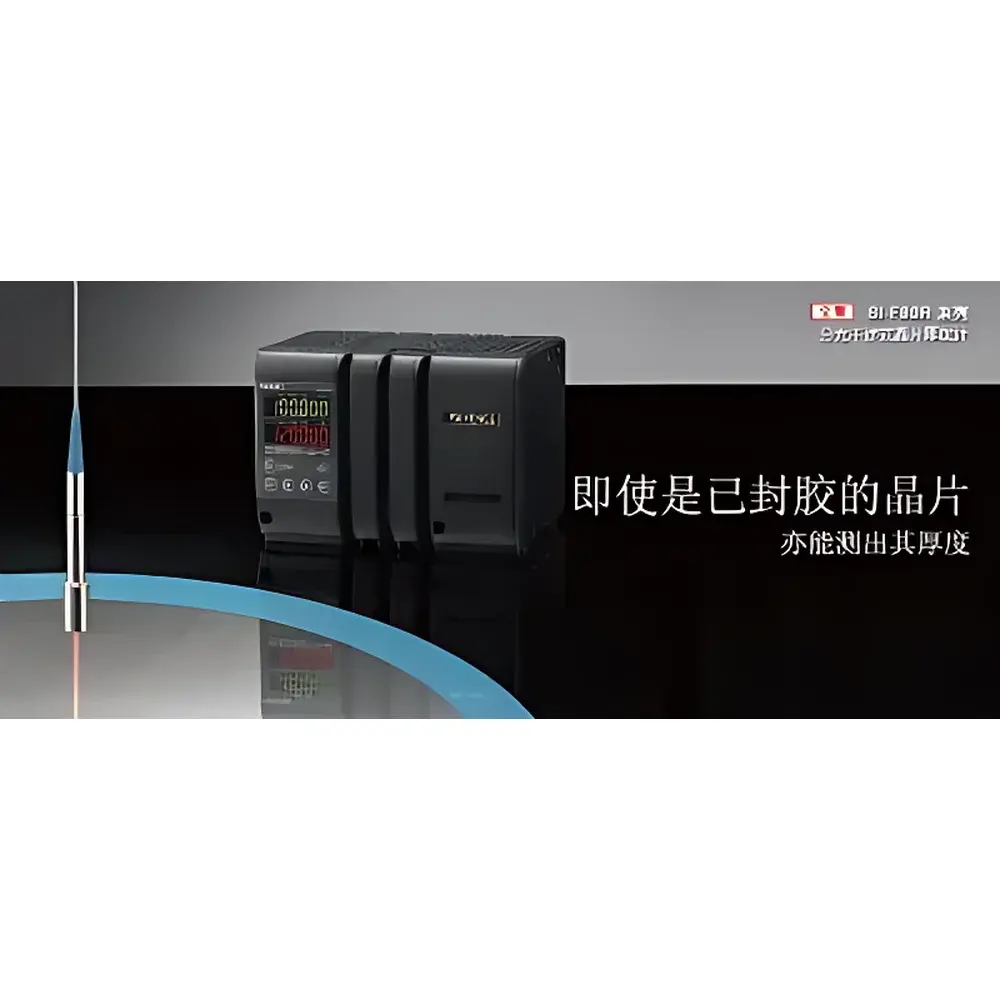
SI-F80R Series Spectral Interferometric Wafer Thickness Gauge
| Origin | Japan |
|---|---|
| Manufacturer Type | Authorized Distributor |
| Origin Category | Imported |
| Model | SI-F80R |
| Pricing | Available Upon Request |
Overview
The SI-F80R Series Spectral Interferometric Wafer Thickness Gauge is an industrial-grade non-contact metrology system engineered for high-precision, real-time thickness measurement of silicon wafers and other transparent or semi-transparent thin-film substrates. Leveraging spectral domain interferometry (SDI), the instrument analyzes wavelength-dependent interference patterns generated by broadband light reflected from both the front and back surfaces of a wafer. This optical principle enables sub-micrometer resolution without physical contact—critical for handling fragile, coated, or encapsulated wafers where mechanical probing would risk damage or contamination. Unlike time-domain OCT or stylus profilometers, SDI offers superior signal-to-noise ratio and stability in production environments, making the SI-F80R suitable for inline process monitoring in semiconductor front-end fabrication, MEMS packaging, and advanced packaging lines where post-encapsulation thickness verification is required.
Key Features
- Non-contact spectral interferometry with no sample preparation or vacuum requirements
- Capable of measuring thickness through epoxy, silicone, or polymer encapsulants—enabling post-sealing QA without decapsulation
- High-speed acquisition: single-point measurement completed in <100 ms, supporting integration into automated handler systems
- Integrated auto-focus and surface detection algorithms compensate for wafer warpage, tilt, and surface reflectivity variations
- Ruggedized optical head designed for cleanroom compatibility (ISO Class 5 compliant enclosure options available)
- Real-time thickness mapping mode supports radial scanning across 200 mm and 300 mm wafers with ≤±0.3 µm repeatability (1σ, under controlled temperature conditions)
Sample Compatibility & Compliance
The SI-F80R accommodates standard silicon wafers (100–300 mm diameter), SOI, glass carriers, sapphire substrates, and compound semiconductors including GaAs and SiC. It supports measurement of multi-layer stacks—such as oxide/nitride/silicon combinations—provided sufficient optical contrast exists between interfaces. The system complies with ISO 14644-1 (cleanroom air cleanliness), IEC 61326-1 (EMC for industrial measurement equipment), and meets the mechanical safety requirements of IEC 60204-1. While not certified for medical device manufacturing per ISO 13485, its data logging architecture supports GLP/GMP-aligned documentation when paired with validated software configurations.
Software & Data Management
The SI-F80R operates via KEYENCE’s proprietary FA-Control Suite v4.x, which provides intuitive calibration workflows, pass/fail threshold configuration, and statistical process control (SPC) charting (X-bar/R, Cpk). All measurement data—including raw spectral interferograms, thickness profiles, and environmental metadata (ambient temperature, humidity timestamp)—are stored in SQLite-based local databases with optional export to CSV, Excel, or OPC UA servers. Audit trail functionality records operator login, parameter changes, and calibration events in accordance with FDA 21 CFR Part 11 requirements when deployed with Windows OS configured for electronic signature enforcement. Remote diagnostics and firmware updates are supported over Ethernet TCP/IP using standard MELSEC-compatible protocols.
Applications
- Final thickness verification of bonded wafers after temporary adhesive lamination or direct bonding
- In-process monitoring of chemical mechanical polishing (CMP) endpoint detection on blanket films
- Thickness uniformity assessment of deposited dielectric layers (e.g., SiO₂, SiNₓ) prior to lithography
- Quality assurance of fan-out wafer-level packaging (FOWLP) substrates following molding compound encapsulation
- Research-grade characterization of epitaxial layer growth kinetics in MBE or CVD reactors (via ex-situ measurement)
- Failure analysis labs performing non-destructive cross-section validation without cleaving or FIB milling
FAQ
Can the SI-F80R measure wafers with anti-reflective coatings or metal layers?
Yes—provided the topmost layer is semi-transparent or has sufficient optical penetration depth at the instrument’s operating wavelength range (650–950 nm). Opaque metal films require alternative techniques such as XRF or eddy current.
Is calibration traceable to NIST or JIS standards?
Calibration uses fused silica reference standards certified to JIS Z 8015; NIST-traceable calibration kits are available as optional accessories with documented uncertainty budgets.
Does the system support integration with SECS/GEM protocols?
Yes—via optional SECS-II/GEM interface module (model SI-F80R-GEM), enabling host communication for factory automation in semiconductor fabs.
What is the minimum measurable thickness for silicon wafers?
The practical lower limit is ~10 µm for single-crystal Si under optimal alignment; thinner membranes (e.g., SOI handle wafers) may require custom optical path optimization.
Can measurements be performed in ambient air, or is nitrogen purge required?
Ambient air operation is fully supported; nitrogen purging is optional and only recommended for environments with high particulate load or moisture-induced spectral drift concerns.