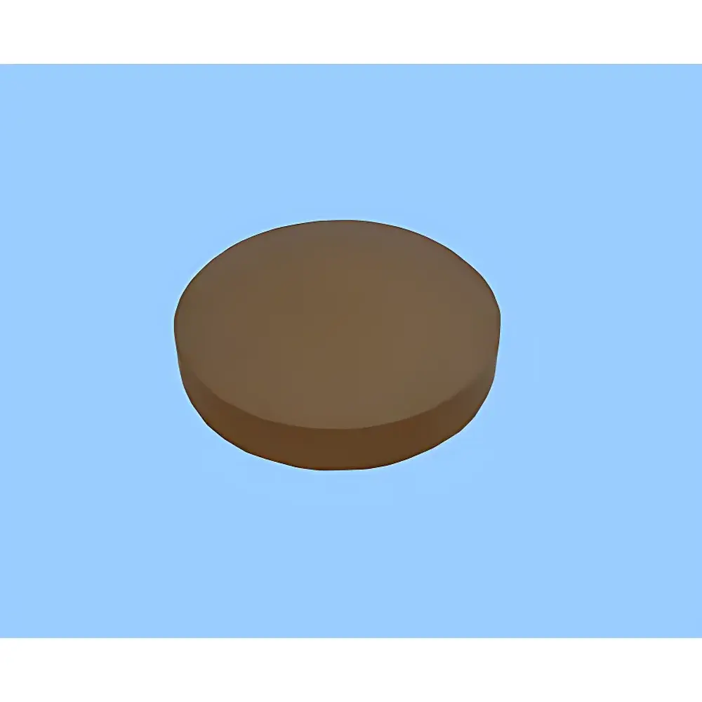
Single-Crystal Sputtering Target | Hefei Kejing Brand
| Brand | Hefei Kejing |
|---|---|
| Origin | Anhui, China |
| Manufacturer Type | Authorized Distributor |
| Origin Category | Domestic (China) |
| Model | Single-Crystal Sputtering Target |
| Pricing | Upon Request |
| Material Purity | 4N–5N (99.99%–99.999%) |
| Relative Density | ≥99.9% TD |
| Max Diameter | Up to 152.4 mm (6") |
| Crystal Orientation Tolerance | ≤0.5° FWHM (XRD rocking curve) |
| Surface Finish | Polished (Ra < 0.5 nm), Optional Double-Sided Lapping |
| Substrate Compatibility | Standard 2.75" / 3.0" / 4.0" / 5.0" / 6.0" CF or Water-Cooled Backing Plates |
Overview
Single-crystal sputtering targets are high-precision evaporation and physical vapor deposition (PVD) materials engineered for applications demanding atomic-level structural coherence, stoichiometric fidelity, and minimal defect density. Unlike polycrystalline or amorphous targets, single-crystal targets eliminate grain boundary scattering, enabling epitaxial thin-film growth with controlled crystallographic orientation—critical for advanced optoelectronic devices, quantum heterostructures, high-frequency acoustic wave resonators, and lattice-matched buffer layers in compound semiconductor fabrication. These targets are grown via the Czochralski (CZ), Bridgman, or floating-zone (FZ) method, followed by precision orientation verification using X-ray diffraction (XRD) Laue back-reflection and rocking-curve analysis. All Hefei Kejing single-crystal targets undergo full crystallographic certification (orientation, mosaicity, and surface plane deviation) and are processed under ISO Class 7 cleanroom conditions to prevent particulate contamination.
Key Features
- Ultra-high purity grades: 4N (99.99%) to 5N (99.999%) elemental and compound compositions, verified by GDMS (Glow Discharge Mass Spectrometry) and ICP-MS trace metal analysis
- Full-density microstructure: ≥99.9% theoretical density (TD), confirmed by Archimedes’ principle and helium pycnometry
- Precise crystallographic alignment: Orientation tolerance ≤0.5° full width at half maximum (FWHM) in XRD rocking curves, with (001), (110), or (111) planes specified per application requirement
- Controlled surface metrology: Double-side polished finish (Ra < 0.5 nm), optional chemical-mechanical polishing (CMP) for ultra-low roughness; flatness ≤1 µm over full diameter
- Thermal and mechanical integrity: Annealed post-machining to relieve residual stress; compatible with DC, RF, and pulsed-DC magnetron sputtering systems up to 5 kW/cm² power density
- Traceability & documentation: Each lot includes a Certificate of Analysis (CoA) with XRD orientation report, density measurement record, purity assay data, and surface roughness profile
Sample Compatibility & Compliance
Hefei Kejing single-crystal targets are designed for integration into standard UHV sputtering chambers (e.g., AJA, Kurt J. Lesker, Denton Vacuum, and custom-built systems). They comply with ASTM F2627–21 (Standard Specification for Single-Crystal Silicon Wafers for Epitaxial Device Applications) and align with ISO/IEC 17025:2017 accredited testing protocols for material certification. For regulated environments—including semiconductor R&D labs operating under IATF 16949 or academic facilities conducting NSF- or DOE-funded thin-film studies—the targets support GLP-compliant documentation workflows. While not inherently FDA-regulated, their manufacturing process adheres to GMP-aligned cleanroom practices (ISO 14644-1 Class 7), and all packaging meets MIL-STD-129R requirements for export-controlled materials.
Software & Data Management
Each target shipment includes a digital CoA delivered as a password-protected PDF with embedded metadata (batch ID, crystallographic orientation vector, date of XRD validation, and GDMS scan summary). Optional integration with laboratory information management systems (LIMS) is supported via CSV or XML export of analytical records. Traceability logs include raw XRD .raw files (Panalytical, Bruker format), surface profilometry (.sur), and density test reports—all archived for ≥10 years per internal quality policy. No proprietary software is required; all data formats conform to ASTM E1392–20 (Standard Guide for Digital Data Exchange in Materials Testing).
Applications
- Epitaxial oxide film growth (e.g., SrTiO₃ on Si for gate dielectrics; LaAlO₃/SrTiO₃ interfaces for 2D electron gas studies)
- High-Q acoustic resonator fabrication (LiNbO₃ and LiTaO₃ for SAW/BAW filters in 5G RF front-end modules)
- Quantum photonic platforms (GaAs and GaP targets for distributed Bragg reflector cavities and quantum dot seeding)
- UV-transparent optical coatings (CaF₂ and MgO for excimer laser optics and synchrotron beamline components)
- Neutron scintillation layer development (Li-containing crystals for thermal neutron detection)
- Substrate-level calibration standards in XRD and TEM sample preparation workflows
FAQ
What crystallographic orientations are available for LiNbO₃ targets?
Standard orientations include Z-cut (001), X-cut (100), and Y-cut (010); custom off-axis cuts (e.g., 128° Y-rotated) are available upon technical review.
Do you provide mounting adapters or bonding services for water-cooled backing plates?
Yes—standard Kovar or CuMo alloy bonding fixtures are offered; indium or AuSn eutectic bonding can be performed per customer-specified thermal cycling protocol.
Is XRD orientation verification performed on every individual target, or only per batch?
100% orientation verification is conducted on each target using automated Laue imaging and rocking-curve mapping prior to final packaging.
Can targets be supplied with pre-deposited seed layers (e.g., TiW adhesion layer)?
No—single-crystal targets are supplied in bare-crystal form to preserve surface stoichiometry and avoid interfacial diffusion during storage; seed layers must be deposited in situ.
What is the typical lead time for 6-inch Si single-crystal targets?
Standard lead time is 8–12 weeks from order confirmation, inclusive of crystal growth, orientation verification, surface finishing, and CoA generation.

 System")

