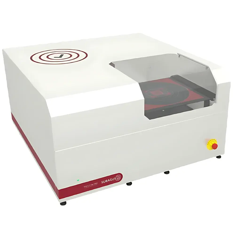
SURAGUS EddyCus TF map 2530 Non-Contact Thin-Film Sheet Resistance and Thickness Mapping System
| Brand | SURAGUS |
|---|---|
| Origin | Germany |
| Model | TF map 2530 |
| Measurement Principle | Non-Contact Eddy Current Sensing |
| Max Scan Area | 300 × 300 mm (12 inch) |
| Sheet Resistance Range | 0.0001–10,000 Ω/□ (with accuracy 2–8% depending on range) |
| Thickness Measurement | 2 nm – 2 mm (for conductive metal layers, e.g., Al, Cu) |
| Spatial Resolution | Adjustable scan step: 1 / 2 / 5 / 10 mm |
| Measurement Density | Up to 1,000,000 points per scan |
| Edge Exclusion | 2 mm standard |
| Max Sample Thickness / Sensor Gap | 2 / 5 / 10 / 25 mm |
| Typical Scan Time | 0.5–5 min (100 × 100 mm), 1.5–15 min (200 × 200 mm) |
| Compliance | ISO/IEC 17025-compatible operation, supports GLP audit trails |
Overview
The SURAGUS EddyCus TF map 2530 is a high-precision, non-contact thin-film characterization system engineered for quantitative mapping of sheet resistance (Rs) and conductive layer thickness across large-area substrates. Based on calibrated eddy current sensing, the instrument operates without physical contact or electrical probing—eliminating risk of surface damage, contamination, or measurement perturbation. It delivers spatially resolved Rs data in Ω/□ and derived metal film thickness in nanometers or micrometers, with traceable calibration against NIST-traceable standards. Designed for R&D laboratories, pilot lines, and quality control environments, the TF map 2530 supports rapid, repeatable evaluation of uniformity, edge effects, defect localization, and process drift—critical for transparent conductive oxide (TCO), sputtered metal grids, printed electronics, and functional coatings used in photovoltaics, display manufacturing, smart glass, and battery current collectors.
Key Features
- Non-contact eddy current mapping with no sample preparation or electrode attachment required
- High-resolution spatial imaging: configurable point density from 10,000 to 1,000,000 measurement points per scan
- Simultaneous dual-parameter output: sheet resistance (0.0001–10,000 Ω/□) and conductive layer thickness (2 nm–2 mm)
- Adjustable scan step size (1, 2, 5, or 10 mm) and programmable scan area up to 300 × 300 mm (12-inch format)
- Automated edge exclusion (2 mm default) and substrate-dependent lift-off compensation
- Multi-range accuracy optimization: ±2–8% depending on Rs magnitude and material conductivity
- Modular sensor head design supporting variable lift-off gaps (2 / 5 / 10 / 25 mm) for thick or warped substrates
- Real-time thermal drift compensation and automatic zero-point recalibration between scans
Sample Compatibility & Compliance
The TF map 2530 accommodates rigid and flexible substrates including float glass, fused silica, polymer foils (PET, PI), silicon wafers, ceramic carriers, and laminated composites. It is validated for use with aluminum, copper, silver, ITO, AZO, FTO, graphene, CNT networks, PEDOT:PSS, and other conductive thin films—regardless of transparency or dielectric backing. All measurements adhere to fundamental electromagnetic principles described in ASTM E1004 (Standard Practice for Determining Electrical Conductivity Using Eddy Current Methods) and support ISO/IEC 17025-compliant uncertainty budgets. The system’s firmware and data export protocols are structured to align with GLP documentation requirements, including timestamped operator ID, instrument configuration logs, and raw signal metadata for full traceability.
Software & Data Management
Controlled via SURAGUS’ proprietary TF Studio software, the TF map 2530 provides intuitive scan setup, real-time visualization of Rs heatmaps, cross-sectional line profiles, statistical distribution analysis (mean, σ, min/max, CV%), and defect thresholding tools. Data exports include CSV, ASCII, and HDF5 formats with embedded metadata (calibration date, sensor ID, environmental conditions). Audit trail functionality records all user actions, parameter changes, and report generations—meeting FDA 21 CFR Part 11 readiness when deployed in regulated GMP environments. Optional API integration enables automated data ingestion into MES or LIMS platforms via RESTful endpoints or OPC UA.
Applications
- Uniformity validation of sputtered ITO/FTO layers in architectural low-emissivity (Low-E) glass production
- Process window qualification for roll-to-roll metal mesh printing on touch sensor films
- Thickness homogeneity assessment of evaporated aluminum heater layers in defrosting automotive glazing
- Rs mapping of laser-scribed interconnects in perovskite and silicon heterojunction PV modules
- Quality gate inspection of CVD-grown graphene on Cu foil prior to transfer
- Batch release testing of conductive polymer anodes in solid-state battery electrodes
- Anisotropy detection in patterned nanowire networks using directional scan vectoring
FAQ
Does the TF map 2530 require electrical contact with the sample?
No. It uses non-contact eddy current induction and requires no probes, electrodes, or surface metallization.
Can it measure through dielectric layers such as SiO₂ or polymer encapsulation?
Yes—provided the total non-conductive layer thickness remains within the sensor’s effective penetration depth (typically < 100 µm for common oxides at 1–10 MHz excitation frequency).
Is calibration traceable to international standards?
Yes. Factory calibration uses NIST-traceable reference standards; users may perform on-site verification with certified Rs check wafers.
What environmental conditions affect measurement stability?
Ambient temperature fluctuations > ±2°C/hour or strong AC magnetic fields (> 10 mG) may impact long-term repeatability; operation in climate-controlled labs (20–25°C, < 50% RH) is recommended.
How is anisotropic conductivity characterized?
By executing orthogonal scan directions (0°/90° or custom angles) and comparing local Rs variance maps—enabling identification of grain orientation effects or directional deposition artifacts.


")