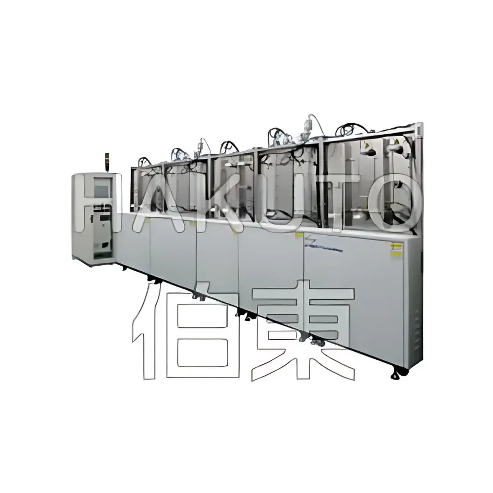
Syskey In-Line Multi-Chamber Magnetron Sputtering System
| Brand | Syskey |
|---|---|
| Origin | Taiwan |
| Manufacturer Type | Authorized Distributor |
| Country of Origin | China (Taiwan) |
| Model | In-Line Sputter |
| Instrument Type | Magnetron Sputtering Deposition System |
| Application Field | Microelectronics |
| Maximum Substrate Size | 1100 × 1300 mm² (glass) |
| Substrate Temperature Range | Up to 400 °C |
| Film Thickness Uniformity | ±5% |
| Ultimate Vacuum | 10⁻⁷ Torr |
Overview
The Syskey In-Line Multi-Chamber Magnetron Sputtering System is an industrial-scale physical vapor deposition (PVD) platform engineered for high-throughput, process-stable thin-film fabrication on large-area substrates. Operating on the principle of magnetron-enhanced plasma sputtering, this system utilizes crossed electric and magnetic fields to confine electrons near the target surface—thereby increasing ionization efficiency, reducing operating pressure, and enabling stable discharge at lower voltages. Unlike batch-type systems, the in-line architecture transports substrates continuously through a sequence of vacuum chambers—each dedicated to a specific process step (e.g., pre-cleaning, sputter deposition, annealing, or in-situ metrology). This configuration ensures excellent inter-run reproducibility, minimizes thermal and mechanical drift, and supports integration into automated semiconductor pilot lines or display manufacturing workflows.
Key Features
- Modular multi-chamber design with independent vacuum isolation between stations—enabling simultaneous process optimization and cross-contamination control.
- Configurable power delivery: RF (up to 5 kW), DC (up to 20 kW), and pulsed DC sources compatible with conductive, semiconductive, and insulating targets (e.g., ITO, SiO₂, AlN, TiN, Cu, Mo).
- Precision substrate handling system supporting glass substrates up to 1100 × 1300 mm²; optional robotic load-lock and conveyor-based transport for integration with front-end lithography tools.
- Active substrate temperature control via embedded heater plates and thermocouple feedback loops—achieving uniform heating up to 400 °C with ±2 °C spatial stability across full substrate area.
- High-accuracy gas distribution manifold with mass flow controllers (MFCs) calibrated for Ar, O₂, N₂, and reactive mixtures—ensuring repeatable stoichiometry in oxide and nitride films.
- Integrated vacuum architecture featuring turbomolecular pumps backed by dry scroll pumps; ultimate base pressure ≤10⁻⁷ Torr, monitored by full-range capacitance manometers and Baratron-controlled pressure regulation.
Sample Compatibility & Compliance
The system accommodates rigid and semi-rigid substrates including soda-lime glass, fused silica, silicon wafers (up to 12-inch equivalent footprint), and flexible metal foils (with appropriate carrier support). All chamber materials conform to ASTM F568M Class 8.8 stainless steel standards, and internal surfaces undergo electropolished passivation to minimize particle generation. The platform meets ISO 14644-1 Class 5 cleanroom compatibility requirements when operated under controlled ambient conditions. Process recipes can be structured to align with SEMI S2/S8 safety guidelines and support GLP-compliant documentation when paired with audit-trail-enabled software (see Software & Data Management section).
Software & Data Management
Control is executed via a real-time Windows-based HMI running deterministic motion and plasma control firmware. The system logs all operational parameters—including voltage, current, pressure, gas flows, temperature profiles, and shutter actuation—with timestamped binary data files compliant with HDF5 format. Optional FDA 21 CFR Part 11–ready software add-ons provide electronic signatures, role-based access control, and immutable audit trails for regulated environments. Integration with third-party MES platforms (e.g., Siemens Opcenter, Applied Materials Envision) is supported via SECS/GEM protocol and OPC UA interfaces.
Applications
- Manufacturing of transparent conductive oxides (TCOs) for touch panels and photovoltaic modules.
- Deposition of gate dielectrics (e.g., Al₂O₃, HfO₂) and metallization stacks in TFT-LCD and OLED backplane development.
- Research-scale synthesis of functional nanolaminates—such as Fe/Cr multilayers for GMR studies or TaN/Ta barriers for advanced interconnects.
- Reactive sputtering of compound films (e.g., TiN, ZnO:Al, SiNx) under precisely controlled partial pressure regimes for optical coating and MEMS packaging.
- In-line process monitoring via optional optical emission spectroscopy (OES) ports or residual gas analyzers (RGA) for endpoint detection and plasma diagnostics.
FAQ
What substrate materials are compatible with this in-line sputter system?
Glass (including alkali-free and low-iron variants), silicon wafers, ceramic substrates, and metal foils—provided they meet flatness and thermal expansion criteria for continuous transport.
Can the system perform reactive sputtering of nitrides or oxides?
Yes—equipped with dual-gas MFCs and real-time pressure feedback, it supports stable reactive deposition of compounds such as Si₃N₄, TiO₂, and AlN using N₂, O₂, or NH₃ precursors.
Is remote diagnostics and preventive maintenance support available?
Syskey provides secure remote access capability for firmware updates, log analysis, and parameter diagnostics—subject to customer network policy and ISO/IEC 27001-aligned cybersecurity protocols.
How is film thickness uniformity validated and maintained?
Uniformity is verified using in-situ quartz crystal microbalances (QCM) and post-deposition ellipsometry mapping; chamber-specific gas distribution tuning and cathode-to-substrate geometry calibration are performed during commissioning.
Does the system comply with semiconductor industry safety standards?
Yes—the platform conforms to SEMI S2 (safety guidelines) and S8 (ergonomics), with CE marking, UL 61010-1 certification, and integrated emergency stop circuits meeting IEC 60204-1 requirements.


