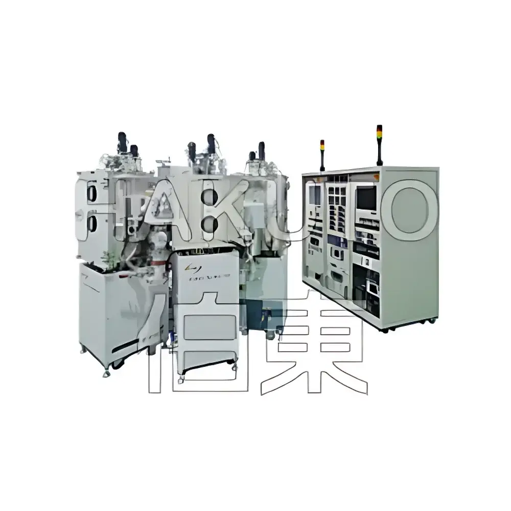
Syskey Organic Material Thermal Evaporation Deposition System
| Brand | Syskey |
|---|---|
| Origin | Taiwan |
| Model | Organic Material |
| Instrument Type | Thermal Evaporation Coater |
| Application Field | Microelectronics |
| Substrate Size | 12-inch (300 mm) wafer or 470 × 370 mm² glass |
| Substrate Temperature Range | Up to 800 °C |
| Film Thickness Uniformity | ±3% |
| Ultimate Vacuum | 5 × 10⁻⁹ Torr |
Overview
The Syskey Organic Material Thermal Evaporation Deposition System is a high-precision, ultra-high vacuum (UHV) physical vapor deposition (PVD) platform engineered for controlled thermal evaporation of organic small molecules and metals onto substrates in research-grade microelectronics laboratories. It operates on the principle of resistive heating—where solid source materials (e.g., Alq₃, NPB, LiF, Ag, Al, MoO₃) are heated in crucibles to their vaporization temperature under UHV conditions, enabling directional condensation onto cooled or heated substrates. The system achieves molecular-level control over deposition kinetics through real-time quartz crystal microbalance (QCM)-based rate monitoring and closed-loop PID temperature regulation of evaporation sources, supporting both sequential and co-evaporation configurations essential for multilayer organic optoelectronic devices.
Key Features
- Ultra-high vacuum chamber constructed from electropolished 304 stainless steel with external water-cooled jacketing and front-loading door equipped with dual borosilicate viewports and manual shutter controls
- 12 independent thermal evaporation sources accommodated within a single chamber—each fitted with motorized shutters, thermocouple feedback, and ±0.1 °C temperature stability via PID controllers
- Crucible compatibility with metal, ceramic, graphite, and pyrolytic boron nitride (PBN) liners—optimized for low-vapor-pressure organics and reactive metals
- Substrate stage supports up to 12-inch (300 mm) wafers or 470 × 370 mm² glass; programmable heating (up to 800 °C) and optional water cooling
- Film thickness uniformity better than ±3% across full substrate area, verified per ASTM F1596 and ISO 14644-1 Class 4 cleanroom-compatible operation
- Integrated residual gas analyzer (RGA) option for in-situ process diagnostics and contamination monitoring
- Modular integration capability with load-lock transfer chambers, robotic handling systems, and inert-atmosphere gloveboxes (N₂ or Ar purged)
Sample Compatibility & Compliance
The system is validated for deposition of thermally stable organic semiconductors (e.g., TPD, α-NPD, CBP), emissive dopants (Ir(ppy)₃, PtOEP), electron/hole transport layers (TPBi, BCP, MoO₃), and reflective electrodes (Ag, Al, Mg:Ag). All wetted components comply with SEMI F57 standards for semiconductor tool materials. Vacuum integrity meets ISO 2859-1 sampling plans for leak-rate validation (<1 × 10⁻¹⁰ mbar·L/s He), and base pressure performance conforms to ASTM E576 classification for Class III UHV systems. Optional RGA and QCM sensors support GLP-compliant data traceability under FDA 21 CFR Part 11 when paired with audit-trail-enabled software.
Software & Data Management
Control is managed via a deterministic real-time operating system (RTOS) interface with synchronized logging of source temperatures, deposition rates (0.01–10 Å/s range), chamber pressure (capacitance manometer + ion gauge), and substrate temperature. All operational parameters are timestamped and exportable in CSV/ASCII format for post-process analysis. Software architecture supports user-defined recipe sequencing—including ramp/soak profiles, shutter coordination logic, and interlock-driven safety protocols (e.g., vacuum interlocks, overtemperature cutoffs). Optional compliance modules provide electronic signature support, change control logs, and role-based access management aligned with ISO/IEC 17025 laboratory accreditation requirements.
Applications
- Development and prototyping of OLED emissive stacks, including RGB pixel architectures and white-light hybrid structures
- Fabrication of organic photovoltaic (OPV) active layers (e.g., P3HT:PCBM bilayers) and interfacial charge transport layers
- Deposition of encapsulation barrier layers (Al₂O₃, SiNₓ, SiOₓNᵧ) via thermal evaporation-assisted ALD precursor delivery
- Research into flexible electronics—enabling low-temperature (<150 °C) deposition on PET and PI substrates using pulsed evaporation modes
- Material screening studies requiring precise stoichiometric control in co-evaporated ternary systems (e.g., host:dopant:exciton blocker)
- Thin-film transistor (TFT) gate electrode and contact layer formation for solution-processed channel layers
FAQ
What vacuum level is required for high-purity organic film deposition?
A base pressure ≤5 × 10⁻⁹ Torr is recommended to minimize hydrocarbon and H₂O partial pressures—critical for preventing oxidation and quenching of triplet excitons in OLED emitters.
Can the system be integrated into a nitrogen-filled glovebox environment?
Yes—standard flange interfaces (CF-63 or CF-100) allow direct connection to gloveboxes with integrated load-lock modules and inert gas purge synchronization.
Is remote monitoring and recipe management supported?
The system supports Ethernet-based OPC UA communication for integration with centralized facility SCADA systems and cloud-based lab informatics platforms.
What maintenance intervals are recommended for the evaporation sources and vacuum pumps?
Crucible cleaning and thermocouple recalibration are advised every 50 operational hours; cryopump regeneration every 200 hours; and turbomolecular pump bearing inspection per ISO 13374 condition monitoring guidelines.
Does the system meet electromagnetic compatibility (EMC) requirements for use in university cleanrooms?
Yes—certified to IEC 61326-1:2023 for laboratory equipment, with conducted/radiated emissions below Class B limits and immunity testing per IEC 61000-4 series.


