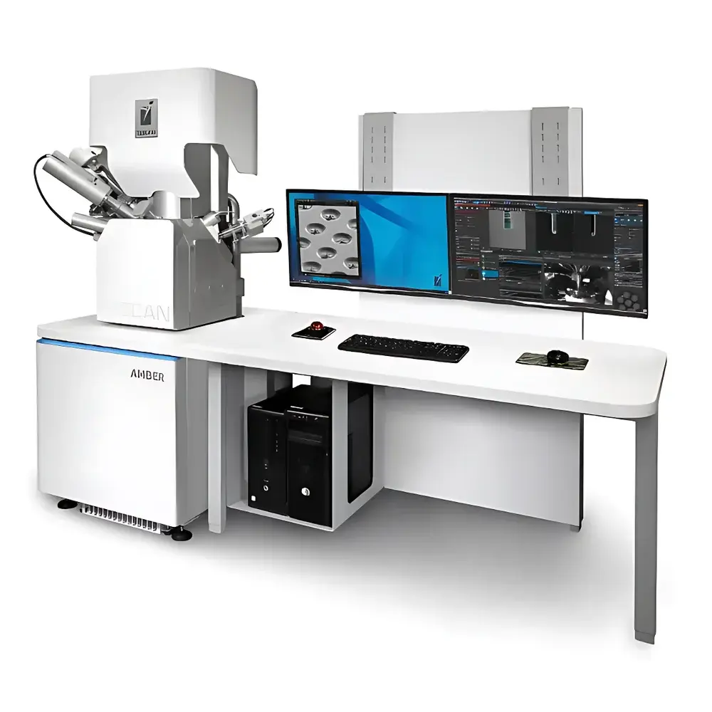
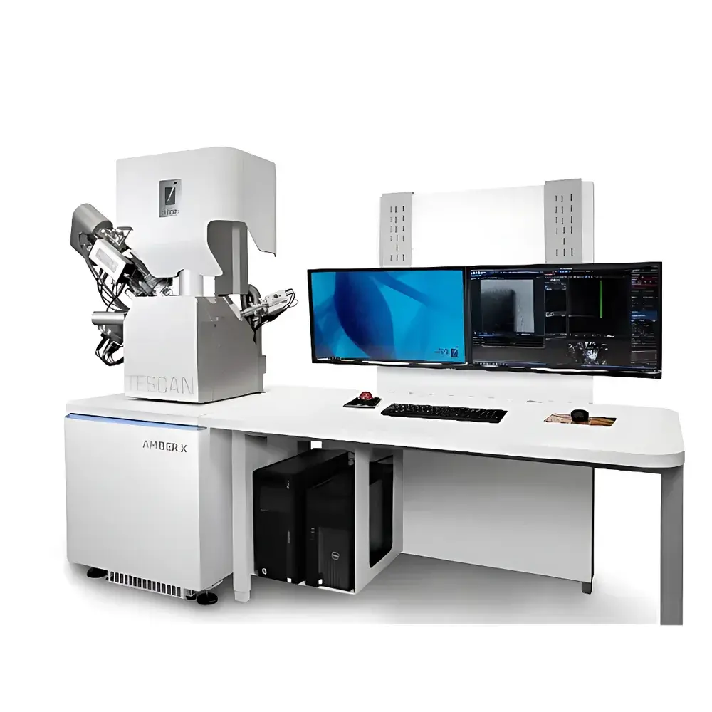
TESCAN AMBER / SOLARIS Dual-Beam Focused Ion Beam Scanning Electron Microscope (FIB-SEM)
| Brand | TESCAN |
|---|---|
| Origin | Czech Republic |
| Model | AMBER / SOLARIS Series |
| Ion Sources | Liquid Metal Ga⁺ & Plasma Xe⁺ |
| Resolution (Xe-FIB) | <15 nm |
| Dual-Beam Alignment | Co-located Electron/Ion Optical Axes |
| Application Domain | Nanofabrication, TEM Lamella Preparation, 3D Microstructural Analysis, Circuit Edit, Failure Analysis |
Overview
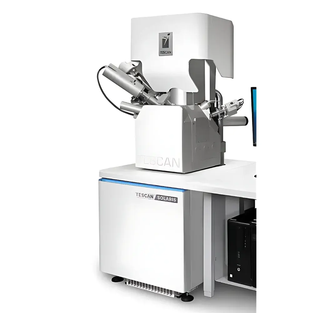
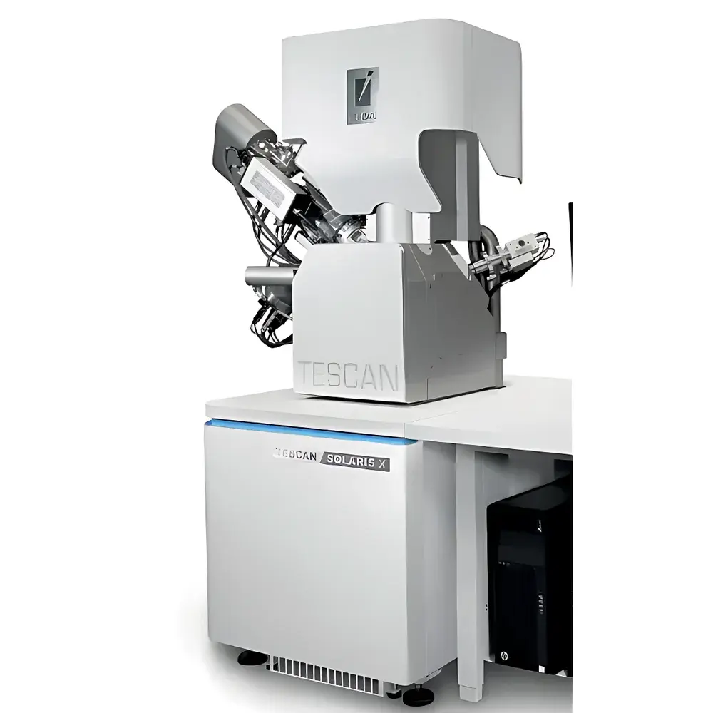
The TESCAN AMBER and SOLARIS series represent high-performance dual-beam focused ion beam scanning electron microscopes (FIB-SEMs), engineered for precision nanoscale imaging, analysis, and in situ fabrication. These systems integrate a thermally assisted field emission scanning electron microscope (SEM) with a high-brightness focused ion beam (FIB) column—either gallium liquid metal ion source (LMIS) or xenon plasma ion source (Xe-PIE)—within a single, rigid vacuum chamber. The co-aligned electron and ion optical axes enable true coincident point operation: the SEM and FIB share a common focal point on the sample surface, permitting real-time, sub-10 nm registration between imaging and milling. This architecture is fundamental to applications requiring iterative nanomachining with immediate feedback—such as site-specific TEM lamella thinning, cross-sectional circuit analysis, and 3D serial sectioning via FIB tomography. Unlike hybrid or add-on FIB attachments, the AMBER/SOLARIS platform features fully synchronized beam control, integrated stage metrology, and hardware-level beam blanking synchronization—ensuring traceable, repeatable, and quantifiable nanofabrication workflows.
Key Features
- Co-registered dual-beam optics with sub-5 nm spatial overlap tolerance between SEM and FIB focal points
- Dual ion source options: High-resolution Ga⁺ LMIS (typical probe size ≤ 7 nm @ 30 kV, 10 pA) and high-current Xe⁺ plasma source (beam current up to 1 µA, enabling material removal rates >50× faster than Ga-FIB)
- Xe-FIB resolution <15 nm at 30 kV (measured per ISO 16700:2014 using knife-edge method), suitable for high-throughput yet high-fidelity nanomachining
- Integrated in-lens SE/BSE detectors, multi-energy backscattered electron (ME-BSE) imaging, and optional energy-dispersive X-ray spectroscopy (EDS) with silicon drift detector (SDD)
- Motorized 5-axis precision stage with laser-interferometric position feedback (repeatability ±25 nm), compatible with cryo-transfer and in-situ heating/cooling holders
- Automated workflow scripting via TESCAN’s Unified Platform software—supporting batch milling, tilt-series acquisition, and recipe-based lamella preparation compliant with ASTM E2961–22 guidelines for TEM specimen preparation
Sample Compatibility & Compliance
The AMBER/SOLARIS platforms accommodate conductive, semi-conductive, and insulating samples up to 150 mm in diameter (standard chamber configuration). Conductive coating (e.g., carbon or platinum sputtering) is optional but not required for most semiconductor or metallurgical specimens due to advanced low-voltage SEM imaging modes (<1 kV) and beam-induced charge compensation. All systems comply with CE marking requirements under the EU Machinery Directive 2006/42/EC and Electromagnetic Compatibility Directive 2014/30/EU. For regulated environments—including semiconductor R&D labs operating under ISO 9001:2015 or device manufacturing facilities aligned with IATF 16949—the instrument supports audit-ready operation logs, user access controls, and electronic signature capability in accordance with FDA 21 CFR Part 11 when paired with validated software configurations.
Software & Data Management
TESCAN’s Unified Platform provides a unified interface for both SEM and FIB operation, eliminating context switching between disparate modules. It includes native support for DICOM-SEM metadata embedding, TIFF-64 export with embedded calibration metadata (pixel size, dwell time, beam energy), and HDF5-based 3D dataset storage for FIB-SEM tomography volumes. Raw image and milling log files are timestamped, checksum-verified, and stored in a hierarchical directory structure compliant with FAIR (Findable, Accessible, Interoperable, Reusable) data principles. Optional integration with Laboratory Information Management Systems (LIMS) is available via RESTful API, enabling traceability from raw acquisition through final report generation in GLP/GMP environments.
Applications
- Transmission electron microscopy (TEM) specimen preparation: Automated lift-out and polishing of site-specific lamellae from IC devices, battery electrodes, and geological thin sections
- Failure analysis in advanced nodes: Cross-sectioning of FinFETs, GAA transistors, and 3D NAND stacks with <20 nm positional accuracy
- 3D microstructural reconstruction: Serial sectioning and reconstruction of multiphase alloys, composite materials, and porous media at voxel resolutions down to 5 nm³
- Nanofabrication & prototyping: Direct-write patterning of plasmonic nanostructures, photonic crystals, and MEMS components using Xe-FIB ablation or Ga-FIB deposition (with precursor gas injection system)
- Materials science correlative workflows: Correlating EDS elemental maps with FIB-milled trenches to quantify grain boundary segregation or phase distribution
FAQ
What is the difference between Ga-FIB and Xe-PIE ion sources?
Ga-FIB delivers superior spatial resolution and fine-feature milling capability, ideal for TEM lamella final polishing and circuit edit. Xe-PIE offers significantly higher ion current (up to 1 µA), enabling rapid bulk material removal while maintaining <15 nm resolution—suited for trenching, via opening, and large-area milling.
Can the system perform automated TEM lamella preparation?
Yes. Predefined, scriptable workflows in Unified Platform support fully automated lift-out, rough milling, thinning, and polishing—including real-time thickness monitoring via electron channeling contrast.
Is the system compatible with cryogenic stages?
All AMBER/SOLARIS models support third-party and TESCAN-integrated cryo-transfer systems for in-situ low-temperature FIB-SEM experiments, including cryo-FIB milling of vitrified biological samples.
How is beam alignment maintained during extended operation?
The system employs active thermal stabilization of optical columns and periodic auto-alignment routines triggered by temperature drift thresholds or user-defined schedules—ensuring long-term beam coincidence stability within ±3 nm over 8-hour sessions.
Does the software support compliance with regulatory documentation standards?
When configured with audit trail logging, electronic signatures, and role-based access control, the Unified Platform meets core requirements of FDA 21 CFR Part 11, ISO/IEC 17025, and EU Annex 11 for computerized systems in regulated laboratories.


