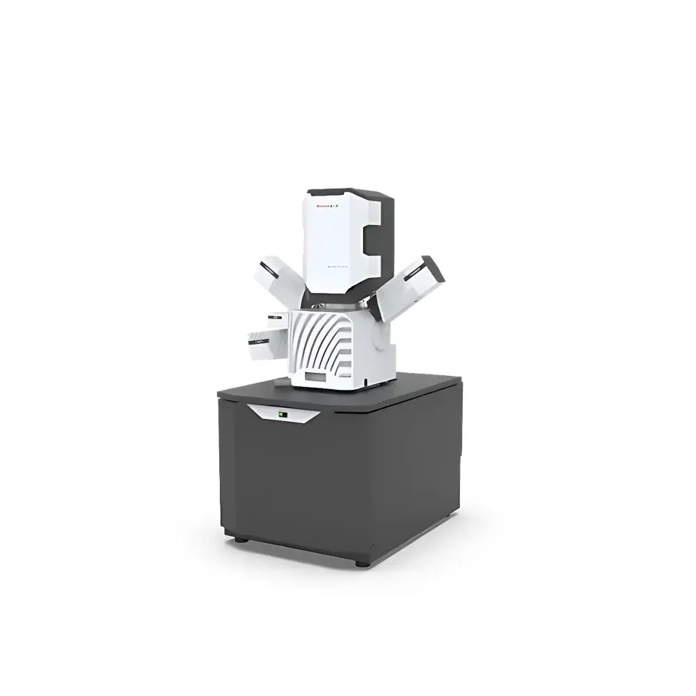
Thermo Fisher Scientific Apreo ChemiSEM Integrated Energy-Dispersive X-ray Spectroscopy Field-Emission Scanning Electron Microscope
| Brand | Thermo Fisher |
|---|---|
| Origin | Guangdong, China |
| Manufacturer Type | OEM Manufacturer |
| Regional Classification | Domestic (China) |
| Model | Apreo ChemiSEM |
| Quotation | Upon Request |
| Instrument Form Factor | Floor-Standing |
| Electron Source Type | Thermal Field-Emission Gun (TFEG) |
| Microscope Class | Ultra-High-Resolution Field-Emission SEM |
| Secondary Electron Resolution | 0.7 nm @ 30 kV |
| Magnification Range | 29× to 200,000× |
| Accelerating Voltage Range | 200 V – 30 kV |
| Backscattered Electron Resolution | 0.8 nm @ 1 kV |
Overview
The Thermo Fisher Scientific Apreo ChemiSEM is an integrated field-emission scanning electron microscope (FE-SEM) engineered for correlative structural, topographic, and compositional analysis at the nanoscale. Leveraging a high-brightness thermal field-emission electron source and a multi-detector architecture optimized for signal separation and collection efficiency, the system delivers sub-nanometer secondary electron (SE) resolution—0.7 nm at 30 kV—and exceptional low-voltage performance with 0.8 nm backscattered electron (BSE) resolution at 1 kV. Its design centers on seamless hardware-software integration, enabling simultaneous acquisition of high-fidelity SE/BSE images, energy-dispersive X-ray spectroscopy (EDS) maps, and crystallographic data without manual reconfiguration. This platform supports both routine quality control and advanced materials research in academic, industrial, and regulatory environments where reproducibility, traceability, and analytical throughput are critical.
Key Features
- Thermal field-emission electron gun (TFEG) providing stable beam current and long-term emission consistency under variable vacuum and voltage conditions.
- Dual-mode imaging capability: high-resolution topographic imaging via in-lens SE detection and compositional contrast via solid-state BSE detectors with atomic number sensitivity.
- Integrated EDS spectrometer with silicon drift detector (SDD), enabling rapid elemental mapping, point-and-click quantification, and phase identification compatible with standard reference libraries (e.g., NIST, JCPDS).
- Variable pressure mode (up to 200 Pa) for direct imaging of non-conductive or hydrated samples without sputter coating.
- Automated stage with 5-axis motorized control (X/Y/Z/tilt/rotation), precision repeatability ±0.1 µm, and programmable multi-location acquisition workflows.
- Real-time beam alignment and stigmation correction via intelligent software algorithms, reducing operator dependency and minimizing setup time per session.
Sample Compatibility & Compliance
The Apreo ChemiSEM accommodates diverse specimen geometries—including bulk metals, ceramics, polymers, geological sections, biological tissues (fixed and dried), and nanomaterials—within a maximum chamber size of Ø200 mm × 120 mm height. Standard sample holders support stubs up to 32 mm diameter; optional holders enable in-situ heating (up to 800 °C), cooling (down to −150 °C), or mechanical straining. All imaging and microanalysis protocols comply with ISO/IEC 17025 requirements for testing laboratories, and EDS quantification workflows align with ASTM E1508 and ISO 22309 standards. Data integrity is ensured through audit-trail-enabled software compliant with FDA 21 CFR Part 11 for electronic records and signatures, supporting GLP and GMP-regulated environments.
Software & Data Management
Operation is managed via Thermo Scientific™ SmartSEM™ software—a unified interface for instrument control, image acquisition, spectral processing, and report generation. The software includes embedded AI-assisted feature recognition for particle analysis, automated grain boundary detection, and layer-thickness measurement tools calibrated against certified reference materials. Raw data (images, spectra, maps) are stored in vendor-neutral formats (TIFF, .emsa, .msa) with embedded metadata (acquisition parameters, calibration history, user ID). Integration with LIMS platforms is supported via OPC UA and RESTful API interfaces. All user actions—including parameter changes, detector selections, and quantification settings—are logged with timestamps and digital signatures for full traceability.
Applications
- Failure analysis of microelectronic interconnects and solder joints using high-magnification BSE imaging coupled with line-scan EDS to identify Cu-Sn intermetallic formation.
- Characterization of battery electrode microstructures, including active material distribution, binder homogeneity, and SEI layer morphology at low-kV conditions to minimize charging artifacts.
- Quality assurance of additive-manufactured metal parts, combining EBSD-based crystallographic orientation mapping with EDS phase identification to verify build integrity and detect porosity-related segregation.
- Forensic analysis of particulate contaminants in pharmaceutical manufacturing environments, where automated particle classification by morphology and chemistry meets USP and ICH Q5A guidelines.
- Nanoparticle dispersion assessment in polymer composites, utilizing statistical particle analysis modules to calculate size distribution, aspect ratio, and spatial clustering metrics.
FAQ
What vacuum levels does the Apreo ChemiSEM support, and how do they affect imaging performance?
The system operates in high vacuum (≤1 × 10⁻⁴ Pa) for maximum resolution and EDS sensitivity, or variable pressure mode (up to 200 Pa) using differential pumping to image uncoated insulators—though with modest resolution trade-offs.
Is the EDS detector cryogen-free, and what is its typical count rate capacity?
Yes—the integrated SDD is Peltier-cooled and rated for >100,000 counts per second (cps) at <1% dead time under standard operating conditions, ensuring accurate quantification even for fast-acquired maps.
Can the Apreo ChemiSEM be upgraded to include EBSD functionality?
Yes—EBSD integration is available as a factory-installed option, including a dedicated phosphor screen, high-speed camera, and OIM Analysis™ software suite for orientation imaging and grain reconstruction.
How is beam damage minimized during long-duration acquisitions on beam-sensitive materials?
Through low-dose imaging modes, dwell time optimization, beam blanking synchronization, and real-time dose monitoring integrated into SmartSEM software—enabling precise control over total electron dose per pixel.
Does the system support remote operation and multi-user access in shared laboratory facilities?
Yes—networked deployment allows secure remote access via TLS-encrypted connections; user roles and permissions are configurable to enforce SOP compliance and prevent unauthorized parameter modification.


