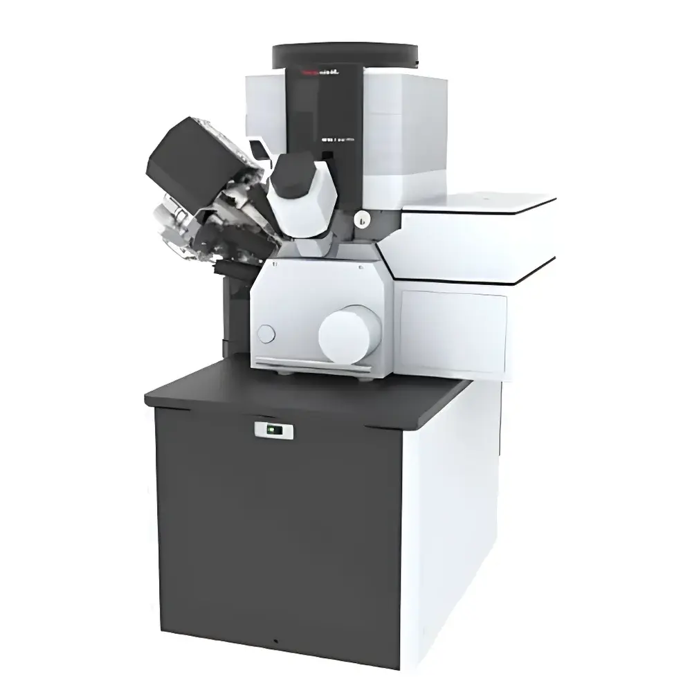
Thermo Fisher Scientific Helios 5 Laser PFIB
| Brand | Thermo Fisher Scientific |
|---|---|
| Origin | Czech Republic |
| Manufacturer Type | Original Equipment Manufacturer (OEM) |
| Origin Category | Imported Instrument |
| Model | Helios 5 Laser PFIB |
| Price Range | USD 920,000 – 1,315,000 |
Overview
The Thermo Fisher Scientific Helios 5 Laser PFIB is a next-generation integrated focused ion beam–scanning electron microscope (FIB-SEM) platform engineered for high-throughput, large-volume 3D nanoscale characterization of materials up to millimeter-scale dimensions. Unlike conventional gallium-based FIB systems, the Helios 5 Laser PFIB uniquely combines three core technologies in a single, co-registered column: a high-performance Elstar™ SEM optics system for sub-nanometer resolution imaging and analytical capabilities (including EDS and EBSD), a plasma-focused ion beam (PFIB) source delivering stable, high-current Ga⁺ or Xe⁺ ion beams across all operational regimes, and a synchronized femtosecond laser ablation system. This tri-modal architecture enables rapid, low-damage, in situ material removal at rates exceeding those of standard Ga-FIB by up to 15,000×—achieving micron-to-hundred-micron depth cuts in under five minutes. The system operates on the principle of hybrid ablation: the ultrafast laser induces controlled thermal stress and phase transition at the surface, while the plasma ion beam precisely mills and polishes the exposed interface, enabling clean, artifact-minimized cross-sections ideal for correlative microscopy and tomographic reconstruction.
Key Features
- Co-axial, fully integrated Elstar™ SEM column with <1.0 nm resolution at 1 kV and high signal-to-noise imaging across low- and high-kV regimes
- Plasma FIB source delivering >100 nA total ion current with stable, long-lifetime Xe⁺ or Ga⁺ operation—enabling uniform milling over mm² areas without beam drift or source degradation
- Femtosecond laser subsystem (center wavelength: ~1030 nm; pulse duration: <400 fs; repetition rate: up to 1 MHz) synchronized to stage motion and ion beam blanking for precise, layer-by-layer ablation
- Automated multi-modal workflow engine supporting unattended overnight 3D serial sectioning, with real-time drift correction and adaptive focus tracking
- Integrated EDS and EBSD detectors compatible with large-area mapping (up to 1 mm × 1 mm) and crystallographic orientation analysis at voxel sizes down to 50 nm
- Advanced sample handling including cryo-transfer capability, charge compensation for insulating samples, and inert-gas lock for air-sensitive materials (e.g., battery cathodes, perovskites, organometallics)
Sample Compatibility & Compliance
The Helios 5 Laser PFIB is validated for use with diverse material classes—including conductive metals, ceramic composites, lithium-ion battery electrodes, optical glasses, polymer blends, thin-film coatings, biological mineralized tissues, and graphene-based heterostructures. Its dual-beam + laser architecture eliminates charging artifacts on non-conductive specimens without requiring conductive coatings, preserving native surface chemistry. For regulated environments, the system supports audit-trail-enabled operation compliant with 21 CFR Part 11 requirements when configured with Thermo Scientific Velox™ Software v4.0 or later. All hardware and software modules conform to ISO 9001-certified manufacturing processes and meet CE/UL safety standards. Routine maintenance protocols align with ASTM E2783 (Standard Guide for FIB Sample Preparation) and ISO/IEC 17025 recommendations for metrological traceability in materials characterization laboratories.
Software & Data Management
Control and analysis are unified through Thermo Scientific Velox™ Software—a modular, Python-extensible platform supporting both interactive operation and automated batch processing. Velox provides real-time 3D reconstruction from serial section datasets, volumetric segmentation using machine learning–assisted thresholding (e.g., U-Net models trained on metallographic and geological datasets), and direct export to industry-standard formats (HDF5, TIFF stack, STL). Data provenance is maintained via embedded metadata (timestamp, beam parameters, stage coordinates, detector settings), and all user actions—including parameter changes and annotation edits—are logged with operator ID and timestamp for GLP/GMP compliance. Remote monitoring and queue management are enabled via Thermo Fisher Connect™ cloud infrastructure, allowing secure access to instrument status, acquisition logs, and raw data archives from external networks.
Applications
- Rapid failure analysis of advanced packaging structures (e.g., TSVs, microbumps) where traditional FIB cannot access subsurface defects within practical timeframes
- Millimeter-scale 3D grain mapping of Ni-based superalloys and additively manufactured Ti-6Al-4V components for microstructure–property correlation studies
- In situ cross-sectional analysis of solid-state electrolyte interfaces in all-solid-state batteries, preserving interfacial chemistry during sectioning
- High-fidelity lamella preparation for S/TEM and atom probe tomography (APT), achieving thickness uniformity <±5 nm across 10 µm × 10 µm areas
- Correlative multimodal imaging workflows integrating PFIB-laser sectioning, EBSD crystallography, and energy-filtered TEM tomography
- Quantitative porosity and phase distribution analysis in porous ceramics and catalyst supports using statistically representative volumes (>10⁶ µm³)
FAQ
What is the primary advantage of the femtosecond laser over conventional FIB milling?
The femtosecond laser enables non-thermal, athermal ablation with minimal heat-affected zone—critical for preserving metastable phases, avoiding recrystallization in amorphous alloys, and preventing decomposition in organic or hydrated samples.
Can the Helios 5 Laser PFIB prepare TEM lamellae directly on silicon nitride membranes?
Yes—its precision laser pre-thinning combined with low-energy PFIB final polishing allows fabrication of electron-transparent regions on suspended membranes with sub-10 nm thickness control and negligible curtaining artifacts.
Is EBSD indexing reliable after laser ablation?
When followed by gentle PFIB polishing (≤5 kV, <10 pA), surface damage is reduced to <2 nm depth, enabling high-confidence EBSD pattern acquisition and orientation mapping comparable to mechanical polishing results.
How does the system handle beam-sensitive biological or polymeric samples?
Through simultaneous low-kV SEM imaging (<1 kV), cryogenic stage cooling (−160 °C), and laser-first ablation strategy, structural integrity is preserved without carbon coating or metal sputtering.
What level of automation is supported for 3D tomography workflows?
Full unattended operation—including auto-focus, auto-stigmation, drift-compensated stage movement, and adaptive slice thickness adjustment—is available via Velox Scripting API and pre-configured application templates.


