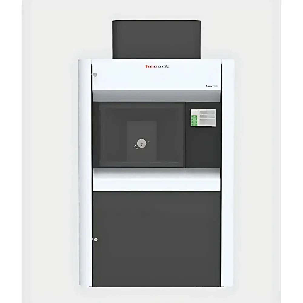
Thermo Fisher Talos F200S G2 Transmission Electron Microscope (TEM)
| Brand | Thermo Fisher |
|---|---|
| Origin | Shanghai, China |
| Manufacturer Type | Authorized Distributor |
| Product Origin | Domestic (China-manufactured under Thermo Fisher global quality system) |
| Model | Talos F200S G2 |
| Price | Upon Request |
| Acceleration Voltage | 200 kV |
| HRTEM Line Resolution | 0.10 nm |
| Minimum Detectable Feature Size | 0.16 nm |
| Field Emission Gun (FEG) Total Beam Current | >150 µA |
| EDS System | Dual in-column SDD Super-X detectors, windowless design with shutter protection |
| EDS Energy Resolution | ≤136 eV at Mn-Kα (10 kcps output) |
| EDS Mapping Pixel Dwell Time | Down to 10 µs |
| EDS Solid Angle | 0.45 sr |
Overview
The Thermo Fisher Talos F200S G2 Transmission Electron Microscope (TEM) is a high-performance 200 kV (scanning) transmission electron microscope engineered for advanced materials characterization in academic, governmental, and industrial research laboratories. Operating on the principles of electron-optical imaging and diffraction, the Talos F200S G2 delivers atomic-scale structural information via high-resolution TEM (HRTEM), scanning TEM (STEM), and integrated energy-dispersive X-ray spectroscopy (EDS). Its column design incorporates a high-brightness Schottky field-emission gun (FEG), enabling stable, high-current electron beams essential for quantitative EDS analysis and time-resolved dynamic experiments. The instrument’s mechanical and thermal stability—enhanced by an active vibration-damping enclosure and environmental compensation architecture—ensures reproducible sub-angstrom imaging across extended acquisition sessions, meeting the stringent requirements of GLP-compliant workflows and ISO/IEC 17025-accredited testing environments.
Key Features
- 200 kV high-voltage platform with ultra-stable FEG source delivering >150 µA total beam current for robust signal-to-noise ratio in both TEM and STEM modes
- HRTEM line resolution of 0.10 nm and point resolution down to 0.16 nm—validated per ASTM E1978 standard for electron microscope resolution assessment
- Dual in-column Super-X SDD EDS detectors with windowless configuration and motorized shutter protection, providing high-collection-efficiency, low-background elemental mapping
- EDS energy resolution ≤136 eV at Mn-Kα (measured at 10 kcps output), compliant with ISO 14707 for microanalysis instrumentation performance verification
- Real-time multi-signal acquisition: simultaneous collection of bright-field (BF), annular dark-field (ADF), high-angle ADF (HAADF), and EDS spectra during STEM scanning
- Velox™ software platform supporting automated acquisition protocols, AI-assisted particle picking, and native support for FAIR data principles (Findable, Accessible, Interoperable, Reusable)
- Modular column architecture enabling on-site upgrade path to Talos F200X configuration—including optional 4D-STEM and in situ heating/cooling stages
Sample Compatibility & Compliance
The Talos F200S G2 accommodates standard 3 mm TEM grids (including SiN membrane, carbon lace, and holey carbon supports) and accepts a wide range of in situ holders—such as electrical biasing, liquid cell, and heating stages (up to 1000 °C)—for operando studies. All hardware and software modules are designed to meet IEC 61000-6-3 (EMC emission) and IEC 61000-6-2 (immunity) standards. Data integrity and audit readiness are ensured through Velox’s built-in 21 CFR Part 11-compliant electronic signature, user role-based access control, and immutable audit trail logging—fully aligned with FDA-regulated QC/QA processes and GMP-aligned analytical development workflows.
Software & Data Management
Velox software serves as the unified interface for instrument control, real-time image processing, spectral quantification, and metadata-rich dataset export. It supports direct integration with Thermo Fisher Connect cloud infrastructure for secure remote collaboration and long-term archival in vendor-neutral formats (e.g., TIFF, MRC, EMDB-compatible HDF5). Batch processing pipelines enable automated drift correction, FFT filtering, and EDS deconvolution using Cliff-Lorimer or ZAF matrix correction models. All raw and processed datasets retain embedded calibration metadata (pixel size, voltage, detector geometry), ensuring traceability per ISO/IEC 17025 Clause 7.5.2 on measurement traceability.
Applications
- Atomic-scale defect analysis in semiconductor heterostructures and battery cathode materials
- Quantitative phase mapping in multiphase alloys and catalyst nanoparticles
- In situ thermal and electrical response monitoring of 2D materials under controlled gas environments
- Correlative microscopy workflows integrating TEM with SEM-EDS, XRD, and Raman data
- Regulatory support for extractables and leachables (E&L) studies in pharmaceutical packaging materials (per USP <1089>)
- Failure analysis of microelectronic interconnects and solder joint reliability assessment
FAQ
What is the difference between Talos F200S G2 and earlier F200S generations?
The G2 iteration features enhanced column vacuum integrity, improved FEG emission stability, upgraded Velox v4.x software with GPU-accelerated reconstruction, and tighter thermal management—resulting in ≥25% improvement in EDS count rate reproducibility over 8-hour sessions.
Is the Talos F200S G2 compliant with FDA 21 CFR Part 11 requirements?
Yes—Velox software includes electronic signatures, audit trail generation, and permission-based user roles validated per Part 11 Annex A guidance for regulated laboratory environments.
Can the system perform quantitative EDS analysis without standards?
It supports both standardless (ZAF/φρz) and standard-based quantification; certified reference materials (e.g., NIST SRM 2100a) are recommended for ISO 14707-compliant reporting.
What sample preparation methods are compatible with high-resolution HRTEM imaging on this system?
Focused ion beam (FIB-SEM) lift-out, electropolishing (for metals), and precision ion milling (for ceramics and composites) are routinely employed to achieve electron-transparent lamellae <100 nm thick.
Does Thermo Fisher provide application support for method development?
Yes—global Application Scientists offer remote and on-site assistance for technique optimization, including STEM tomography, 4D-STEM strain mapping, and in situ protocol validation.


