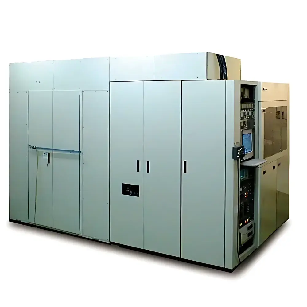
ULVAC IMX-350 Low-Energy, High-Current Ion Implanter
| Brand | ULVAC KIKO |
|---|---|
| Origin | Japan |
| Model | IMX-350 |
| Product Type | Low-Energy, High-Beam-Current Implanter |
| Implantation Energy | 50 keV |
| Dose Range | 1×10¹⁶ ions/cm² |
| Wafer Size | 6-inch |
| Implant Species | p⁺ (Boron, Phosphorus, Arsenic compatible) |
| Beam Current Capability | High-current configuration |
| Ion Source Options | Liquid Metal Ion Source (LMIS), Dual Plasma Source (for O⁺, N⁺), Mass Analyzer Column |
| Imaging Resolution | 4 nm (dual-beam SEM column) |
| Positioning Accuracy | ≤20 nm (with piezo-driven stage and 1 nm optical encoder) |
Overview
The ULVAC IMX-350 is a low-energy, high-current ion implanter engineered for precision dopant introduction in advanced semiconductor process development and quantum device fabrication. Operating on electrostatic acceleration and magnetic mass separation principles, the system delivers controlled, shallow-depth ion implantation with sub-20 nm lateral placement reproducibility. Designed specifically for 6-inch wafers, the IMX-350 integrates a compact, vacuum-integrated architecture optimized for cleanroom deployment and integration into R&D or pilot-line environments. Its 50 keV maximum acceleration voltage enables ultra-shallow junction formation—critical for FinFET, nanowire transistors, and silicon-based qubit structures—while maintaining high beam current stability for throughput-sensitive processes such as blanket doping or selective-area implantation.
Key Features
- Low-energy, high-current ion optics: Optimized extraction and focusing optics support stable beam currents up to several hundred microamperes at 50 keV, enabling rapid dose delivery with minimal thermal load on sensitive substrates.
- Nanopositioning stage: Piezo-driven XY stage equipped with 1 nm resolution optical encoders ensures repeatable, drift-compensated sample positioning—essential for single-ion or multi-species site-specific implantation.
- Multi-source ion generation: Configurable with Liquid Metal Ion Source (LMIS) for high-brightness, mono-isotopic beams (e.g., Ga⁺, In⁺, Bi⁺), and dual plasma source options for reactive species including O⁺ and N⁺—supporting both dopant and passivation implantation.
- Mass-analyzed beam delivery: Integrated 90° magnetic sector mass analyzer provides isotopic purity >99.9% for critical dopants such as ¹¹B⁺, ³¹P⁺, and ⁷⁵As⁺, minimizing contamination from molecular or charge-state contaminants.
- In-situ imaging and verification: Dual-beam electron column (SE + BSE detection) delivers real-time 4 nm resolution imaging, enabling immediate post-implant inspection, alignment verification, and process feedback without breaking vacuum.
- Modular vacuum architecture: All-metal, UHV-compatible construction with turbomolecular pumping achieves base pressure <5×10⁻⁸ Pa, ensuring minimal residual gas interaction during low-energy beam transport.
Sample Compatibility & Compliance
The IMX-350 accommodates standard 6-inch silicon, SiC, GaN, and SOI wafers with manual or semi-automated load-lock operation. Chuck temperature control (−50 °C to +150 °C) mitigates channeling effects and enables cryogenic implantation for enhanced damage confinement. The system conforms to ISO 14644-1 Class 5 cleanroom requirements and supports integration with factory automation interfaces (SECS/GEM). Full audit trail logging, user-access controls, and electronic signature capability align with GLP and FDA 21 CFR Part 11 readiness for regulated R&D environments.
Software & Data Management
Controlled via ULVAC’s proprietary ImplantStudio™ platform, the IMX-350 offers scriptable recipe management, real-time beam current and dose monitoring with ±0.5% linearity, and automated calibration routines for energy and dose verification. All process parameters—including source settings, mass analyzer tuning, stage coordinates, and imaging metadata—are time-stamped and stored in SQLite-based local databases. Export formats include CSV, HDF5, and industry-standard SECS-II logs for traceability and statistical process control (SPC) integration.
Applications
- Quantum device fabrication: Single-ion implantation for NV-center creation in diamond, phosphorus donor arrays in silicon, and deterministic qubit placement.
- Advanced CMOS process development: Ultra-shallow junctions, halo implants, and retrograde profiles for sub-5 nm node feasibility studies.
- Nanophotonic structure engineering: Localized refractive index modification in SiN or TiO₂ waveguides via controlled dopant gradients.
- Novel memory devices: Oxygen vacancy engineering in HfO₂-based RRAM, nitrogen doping in IGZO TFT channels.
- Materials science research: Controlled defect engineering in 2D materials (MoS₂, h-BN) and wide-bandgap semiconductors (AlN, Ga₂O₃).
FAQ
What ion species are supported by the IMX-350?
The system supports p⁺ dopants (B⁺, P⁺, As⁺) as standard, with optional LMIS for Ga⁺, In⁺, Bi⁺, and dual plasma sources for O⁺ and N⁺.
Is the IMX-350 suitable for production use?
It is configured for R&D and pilot-line applications; throughput and automation level are optimized for flexibility and process learning—not high-volume manufacturing.
Can the system perform angle-tilted implantation?
Yes—programmable wafer tilt (±15°) and rotation enable channeling suppression and anisotropic profile control.
Does ULVAC provide installation and qualification support?
Yes—comprehensive IQ/OQ documentation, vacuum leak testing, beam alignment certification, and operator training are included in standard commissioning.
How is beam uniformity verified?
Uniformity mapping is performed using a Faraday cup array or calibrated silicon diode scanner; typical 1σ non-uniformity across 6-inch wafers is ≤2.5% for p⁺ at 50 keV.


