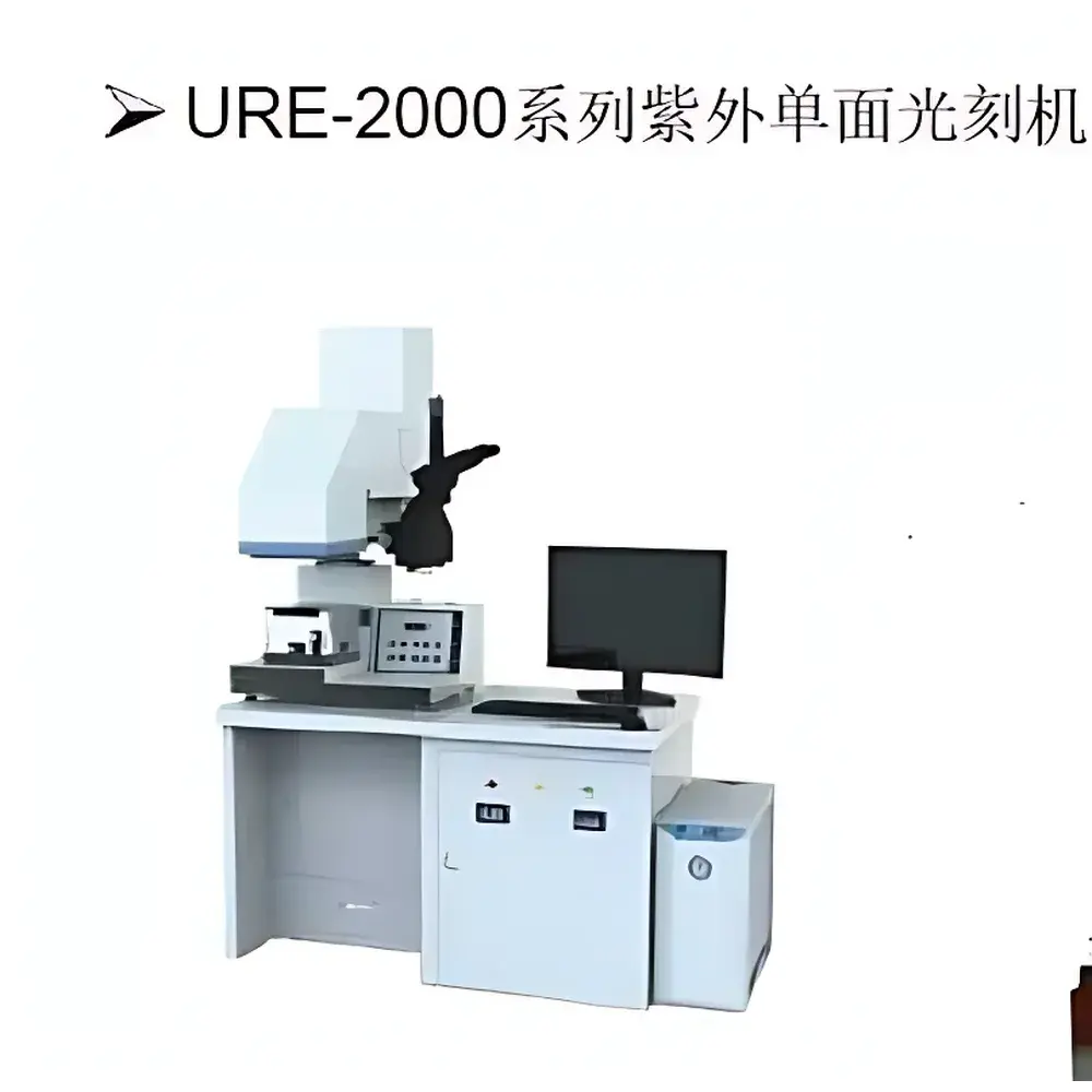
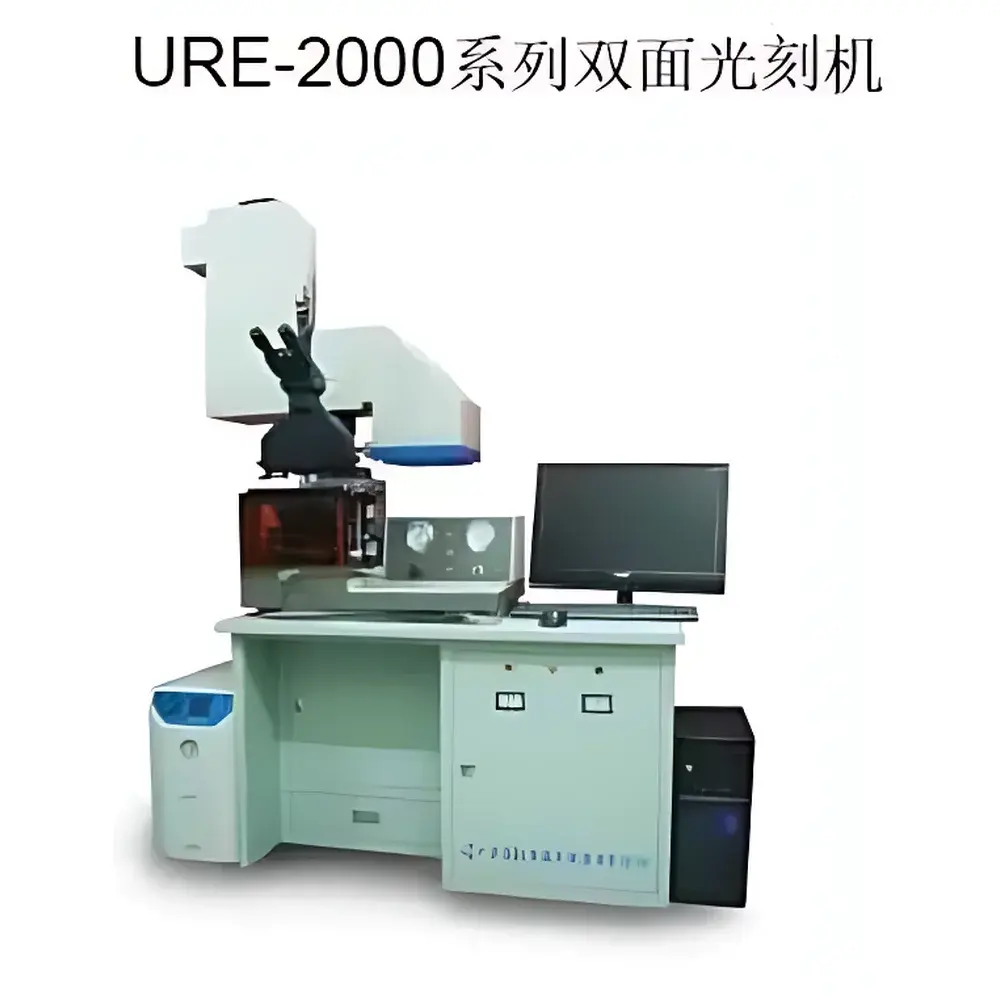
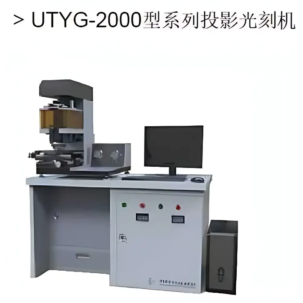
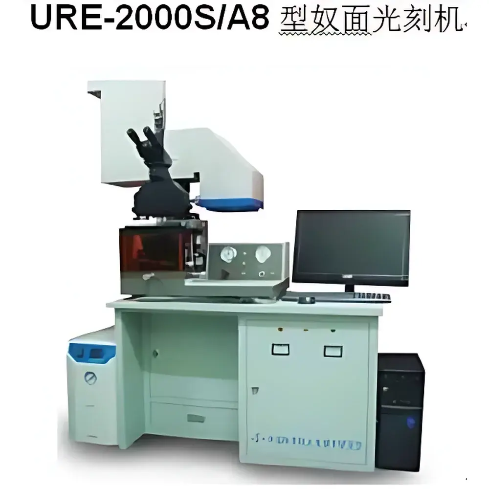
URE-2000 Series UV Contact and Proximity Mask Aligner for Microarray and Semiconductor Microfabrication
| Origin | Sichuan, China |
|---|---|
| Manufacturer Type | Authorized Distributor |
| Origin Category | Domestic (China) |
| Model | URE-2000 Series |
| Price Range | USD 42,000 – 70,000 |
| Scanning Throughput | 2 µm feature resolution |
| Resolution | 0.8 µm (with 2 µm positive photoresist) |
| Detection System Type | UV Optical Detection |
| Excitation Wavelength | 365 nm (i-line) |
| Emission Wavelength | 365 nm |
| Exposure Area | Up to 200 mm × 200 mm (URE-2000/A8) |
| Exposure Time Range | 0.1 s – 9999.9 s (programmable timer) |
| Mercury Lamp Power | 1000 W (DC, Osram Ultra-High-Pressure Hg Lamp) |
| Illumination Uniformity | ≤2.5% (Ø100 mm), ≤5% (Ø200 mm) |
| Alignment Accuracy | ±0.8 µm (single-side), ±2 µm (double-side, 0.8 mm wafer thickness) |
| Maximum Resist Thickness | 500 µm (SU-8, user-provided conditions) |
Overview
The URE-2000 Series UV Contact and Proximity Mask Aligner is a precision-engineered optical lithography platform designed for research-grade microfabrication in life science chip development, microarray manufacturing, MEMS prototyping, and academic semiconductor process labs. Unlike projection or stepper-based systems, the URE-2000 operates on the principle of near-field contact or proximity exposure using collimated i-line (365 nm) illumination from a stabilized DC-driven ultra-high-pressure mercury lamp (Osram). Its core architecture integrates a patented “modular offset fly’s-eye lens” array to suppress diffraction effects and enhance sidewall verticality—critical for high-fidelity patterning of biomolecular capture zones, electrode arrays, and microfluidic channel definitions. The system supports both single- and double-sided alignment via real-time CCD imaging of substrate backside features, enabling accurate registration for stacked biochip architectures without requiring expensive backside metallization. With exposure fields scalable from 100 mm × 100 mm (TYG-2000 variants) up to 200 mm × 200 mm (URE-2000/A8), it bridges the gap between benchtop R&D and pilot-line fabrication under controlled environmental conditions.
Key Features
- Modular fly’s-eye illumination optics delivering ≤2.5% intensity non-uniformity over Ø100 mm and ≤5% over Ø200 mm—meeting ISO 9022-3 illumination homogeneity requirements for reproducible dose delivery.
- CCD-based bottom-side alignment with real-time image overlay, enabling sub-micron registration accuracy without reliance on front-side fiducials alone.
- Multi-mode exposure control: vacuum contact, hard contact, soft pressure contact, and proximity gap (10–50 µm adjustable) — fully configurable per process recipe.
- Dual-stage motion system: coarse mask/sample translation (X/Y ±10 mm) and fine relative alignment (X/Y ±5 µm, θ ±6°) with micrometer-level repeatability.
- Integrated water-cooled lamp housing maintaining thermal stability at the exposure plane (<±0.5 °C drift during 60-min operation), minimizing focus drift and pattern distortion.
- Nanoprinting interface compliant with standard PDMS stamp mounting protocols, allowing hybrid lithography workflows combining UV exposure and soft lithography.
- DC-powered 1000 W Osram HBO mercury lamp with daily automatic intensity calibration referenced to 356 nm output, ensuring long-term dose stability across multi-day experiments.
Sample Compatibility & Compliance
The URE-2000 Series accommodates substrates ranging from 1-inch wafers to 8-inch (200 mm) silicon, glass, quartz, or polymer chips—including irregular fragments and flexible PET-based microarrays. Standard chuck configurations include vacuum-suction flat stages with anti-reflective surface coating to minimize standing-wave interference in thick resist films. Mask compatibility spans 3″, 5″, 7″, and 9″ formats with precision kinematic clamping. All exposure modes comply with ASTM F1247-22 (Standard Practice for Photolithographic Process Control) and support GLP/GMP-aligned documentation when integrated with optional audit-trail software modules. The 365 nm i-line source conforms to IEC 62471 photobiological safety classification for Class 3R UV equipment, with interlocked chamber access and real-time UV intensity monitoring.
Software & Data Management
The native control suite provides ISO/IEC 17025-compliant exposure parameter logging—including timestamped lamp intensity readings, stage coordinates, exposure duration, and user-defined recipe IDs. Optional FDA 21 CFR Part 11 compliance packages deliver electronic signature support, role-based access control, and immutable audit trails for regulated life science applications. Real-time graphical display shows active exposure zone, remaining time, accumulated dose (mJ/cm²), and thermal drift compensation status. Export formats include CSV, XML, and HDF5 for integration into LIMS or statistical process control (SPC) platforms. Remote monitoring via Ethernet TCP/IP enables centralized lab fleet management without compromising local operational security.
Applications
- Microarray substrate fabrication: high-density DNA, protein, and glycan chip patterning with <1 µm feature fidelity on functionalized glass slides.
- Lab-on-chip device prototyping: definition of microelectrode arrays, microfluidic channel networks, and integrated sensor pads in SU-8, AZ, or PMMA resists.
- MEMS packaging alignment: double-sided lithography for through-silicon via (TSV) registration and cap wafer bonding alignment.
- Optical biosensor development: fabrication of grating-coupled surface plasmon resonance (SPR) and photonic crystal slabs requiring sub-500 nm linewidth control.
- Academic microfabrication training: hands-on instruction in photomask handling, exposure dose optimization, resist development kinetics, and alignment metrology.
FAQ
What resist thicknesses are supported?
The system supports photoresists from 0.5 µm to 500 µm, validated with SU-8, AZ series, and Shipley S1800 resists. Maximum thickness depends on exposure energy density and developer compatibility—users must provide process-specific validation data.
Is the 365 nm source filtered to exclude UV-C or visible emission?
Yes. A cold mirror dichroic filter and fused silica condenser assembly suppress wavelengths below 350 nm and above 400 nm, delivering >92% spectral purity at 365 nm per IEC 61228 specifications.
Can the system be upgraded for double-sided alignment?
All URE-2000/A8 and URE-2000S models include native CCD-based bottom-side imaging; no hardware retrofit is required—only software license activation and alignment target calibration.
Does the aligner meet cleanroom compatibility standards?
The frame is constructed from anodized aluminum and stainless steel with non-outgassing elastomers. It complies with ISO Class 5 (Class 100) cleanroom operational guidelines when used with HEPA-filtered air supply and static-dissipative flooring.
What maintenance intervals are recommended for the mercury lamp?
Lamp lifetime is rated at ≥1,200 hours at rated power. Intensity calibration is performed automatically each startup; full lamp replacement is advised after 1,000 hours or if output drops >10% below baseline per quarterly spectroradiometric verification.