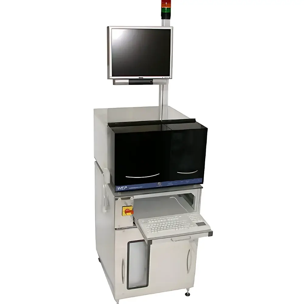
WEP CVP21 Electrochemical Capacitance-Voltage Profiler
| Brand | WEP |
|---|---|
| Origin | Germany |
| Model | CVP21 |
| Measurement Principle | Electrochemical Capacitance–Voltage (ECV) Profiling |
| Carrier Concentration Range | 1×10¹¹ to 1×10²¹ cm⁻³ |
| Depth Resolution | Down to ≤1 nm |
| Compatible Substrates | Conductive & insulating |
| Wafer Size Support | 4×2 mm² to 200 mm (8″) |
| Material Compatibility | Si, Ge, SiC, GaAs, InP, GaN, AlGaN, InGaN, AlInN, ZnO, CdTe, HgCdTe, and multicomponent III–V/II–VI compounds |
| Automation Level | Fully automated with real-time corrosion monitoring, dry-in/dry-out handling, and camera-assisted process control |
Overview
The WEP CVP21 Electrochemical Capacitance–Voltage Profiler is a precision metrology instrument engineered for quantitative depth-resolved carrier concentration profiling in semiconductor epitaxial layers, diffusion junctions, and ion-implanted structures. Based on the electrochemical capacitance–voltage (ECV) technique, the system measures the differential capacitance of a semiconductor/electrolyte junction as a function of applied bias voltage. By sequentially electrochemically etching the surface layer-by-layer while acquiring capacitance–voltage data at each step, the CVP21 reconstructs vertical dopant distribution profiles with sub-nanometer depth resolution. This method is fundamentally distinct from solid-state CV or SIMS, offering direct correlation between electrical activity and spatial location without requiring sputter calibration standards or matrix effects correction. The CVP21 is widely deployed in R&D laboratories and process development fabs for compound semiconductor optimization—including wide-bandgap materials such as GaN, SiC, and AlGaN—where traditional techniques face limitations due to low carrier mobility, high resistivity, or surface recombination artifacts.
Key Features
- Modular, cleanroom-compatible architecture with physically isolated optical, electronic, and fluidic subsystems—ensuring long-term stability and minimizing cross-contamination risk.
- Self-calibrating measurement electronics with automatic compensation for cable capacitance, electrode polarization, and electrolyte resistance drift—eliminating routine user recalibration.
- Real-time, color-camera-monitored etching process: integrated optical imaging captures surface morphology before, during, and after each etch step; image metadata is time-stamped and archived with raw C–V datasets.
- Dry-in/dry-out sample handling: fully automated electrochemical cell loading, unloading, and repositioning via programmable XYZ stage—enabling repeatable positioning for multi-site analysis on large wafers.
- Predefined measurement templates with editable priority-based sequencing—supporting standardized test protocols for QC environments while allowing R&D users to define custom voltage sweep rates, etch durations, and stop criteria.
- Robust fluid management system with closed-loop electrolyte circulation, temperature stabilization (±0.1 °C), and inert-gas purging—critical for reproducible etching kinetics across air-sensitive materials like InGaN or HgCdTe.
Sample Compatibility & Compliance
The CVP21 supports a broad spectrum of semiconductor material systems without substrate conductivity constraints: both conductive (e.g., heavily doped Si, n-GaN) and insulating substrates (e.g., sapphire, SiO₂/Si, Al₂O₃) are compatible. It accommodates samples ranging from small diced chips (4 × 2 mm²) to full 200 mm (8″) wafers. Material coverage includes elemental semiconductors (Si, Ge), IV–VI compounds (SiC), III–V binaries (GaAs, InP), ternaries (AlGaAs, InGaP), quaternaries (AlGaInP), nitrides (GaN, AlGaN, InGaN, AlInN), II–VI compounds (ZnO, CdTe, HgCdTe), and emerging chalcogenides. All measurements comply with ASTM F1188–22 (“Standard Practice for Determining Semiconductor Dopant Profiles by Electrochemical Capacitance–Voltage Profiling”) and support GLP/GMP audit readiness through full electronic record retention, user-access logging, and 21 CFR Part 11–compliant software configuration (optional validation package available).
Software & Data Management
The CVP21 operates under WEP’s proprietary ProfilSoft™ platform—a Windows-based application built on .NET Framework with deterministic real-time task scheduling. The software provides synchronized control of potentiostat sweeps, motorized stage movement, camera acquisition, and electrolyte flow rate. All raw data—including analog capacitance traces, digital etch depth counters, thermal sensor logs, and timestamped images—are stored in vendor-neutral HDF5 format with embedded metadata (user ID, timestamp, calibration hash, instrument firmware version). Batch processing tools enable automated profile extraction using standard Debye–Hückel and Mott–Schottky models; output files export directly to CSV, MATLAB (.mat), or industry-standard SECS/GEM formats. Audit trails record every parameter change, measurement start/stop event, and software update—fully traceable for ISO 9001 and IATF 16949 quality system requirements.
Applications
- Epitaxial layer characterization: quantification of doping gradients, interface abruptness, and background carrier density in MOCVD- or MBE-grown heterostructures.
- Ion implantation process validation: verification of projected range (Rp), straggle (ΔRp), and activation efficiency in annealed implants.
- Junction depth metrology: determination of metallurgical junction depth (xj) in diodes, HBTs, and power devices—correlatable with spreading resistance probe (SRP) and secondary ion mass spectrometry (SIMS).
- PEC etch development: in-situ optimization of photoelectrochemical etch selectivity and surface passivation for GaN-based UV LEDs and laser diodes.
- Failure analysis: root-cause investigation of leakage paths, dopant segregation, or interfacial oxidation in high-k/metal gate stacks.
- Process transfer support: generation of reference profiles for technology node migration between pilot line and high-volume manufacturing.
FAQ
What electrolytes are required for different semiconductor materials?
Electrolyte selection is material-specific and optimized for controlled anodic dissolution without surface pitting or preferential etching. Standard formulations include HF-based solutions for Si and SiC, HCl/HBr mixtures for III–V compounds, and buffered ammonium hydroxide for ZnO. WEP provides validated electrolyte recipes and compatibility matrices upon request.
Is the CVP21 suitable for production-line integration?
Yes—the system supports SEMI E10-compliant equipment interfaces, recipe-driven operation, and statistical process control (SPC) data export. Optional hardware kits enable integration with FOUP load ports and factory MES systems via SECS/GEM.
How does the CVP21 handle insulating substrates like sapphire or quartz?
A conductive backside contact (e.g., evaporated Au or Ni film) is applied prior to measurement. The system’s high-input-impedance potentiostat ensures accurate C–V acquisition even with series resistance >10⁶ Ω.
Can depth resolution be improved beyond 1 nm?
Achievable resolution depends on etch uniformity, surface recombination lifetime, and electrolyte mass transport. For ultra-thin layers (<5 nm), pulsed etching modes and low-bias sweep rates can yield effective resolution down to ~0.3 nm in optimized GaN-on-sapphire structures.
Does WEP provide application support for novel materials not listed in the datasheet?
Yes—WEP maintains an open-sample evaluation program. Qualified researchers may submit representative samples for feasibility testing; results include full profile plots, uncertainty analysis per GUM guidelines, and recommended measurement parameters.


