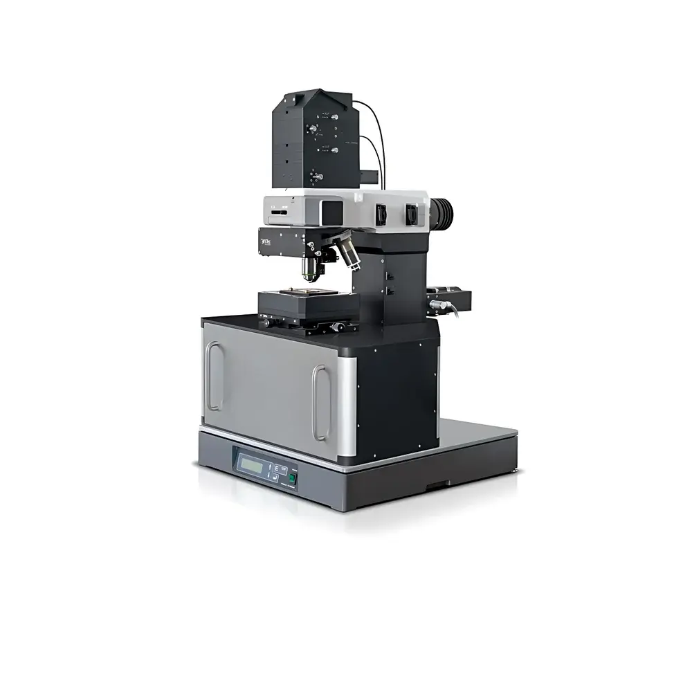
WITec alpha300S Scanning Near-Field Optical Microscope (SNOM)
| Brand | Oxford Instruments |
|---|---|
| Country of Origin | Germany |
| Model | alpha300S |
| Detection Principle | Aperture-type Scanning Near-Field Optical Microscopy (SNOM) |
| Lateral Resolution | ~60 nm |
| Operating Modes | Transmission & Reflection |
| Compatible Detectors | High-sensitivity PMT & APD with overload protection |
| Integrated Spectroscopy | UHTS spectrometer compatible |
| Multimodal Capabilities | Combined AFM, Confocal Microscopy, and SNOM |
| Environmental Operation | Ambient air and liquid environments |
| Sample Preparation | Label-free, non-destructive, minimal preparation required |
| Upgrade Path | Optional integration with confocal Raman and near-field Raman imaging |
Overview
The WITec alpha300S is a high-performance scanning near-field optical microscope (SNOM) engineered for label-free, non-invasive nanoscale optical imaging beyond the diffraction limit. Unlike far-field super-resolution techniques such as STED or STORM—which rely on photoactivatable fluorophores, complex illumination schemes, and photostability constraints—the alpha300S operates on aperture-based near-field detection, enabling direct spatial mapping of optical properties at ~60 nm lateral resolution without molecular labeling. Its core principle leverages evanescent field coupling through a metal-coated, tapered optical fiber probe scanned in close proximity (<10 nm) to the sample surface. This architecture ensures consistent sub-diffraction resolution across diverse material classes—including dielectrics, semiconductors, 2D materials, biological membranes, and plasmonic nanostructures—without dependence on fluorescence quantum yield or photobleaching resistance.
Key Features
- Patented SNOM probe technology with integrated shear-force feedback for stable, drift-compensated operation in both ambient air and aqueous environments.
- Simultaneous multimodal acquisition: synchronized topographic (AFM), far-field optical (confocal), and near-field optical (SNOM) data within a single scan cycle.
- Automated tip approach and optimization routines controlled via WITec’s proprietary control software, minimizing operator dependency and improving measurement reproducibility.
- Dual-detector configuration supporting either high-gain photomultiplier tube (PMT) or avalanche photodiode (APD) with real-time overload protection—critical for handling dynamic signal ranges typical in heterogeneous samples.
- Modular optical path design allowing seamless integration of the UHTS (Ultra-High Throughput Spectrometer) for point-spectral or hyperspectral near-field imaging (nano-FTIR and nano-PL capabilities).
- Scalable platform architecture: factory-upgradeable to confocal Raman microscopy and tip-enhanced Raman scattering (TERS), enabling correlative nanoscale chemical identification alongside topography and optical contrast.
Sample Compatibility & Compliance
The alpha300S supports a broad range of uncoated, unstained, and unmodified specimens—including live cells in buffered solution, graphene monolayers on SiO₂/Si substrates, polymer blends, photonic crystals, and catalytic nanoparticles. Its non-contact, low-force AFM mode (typically <50 pN) preserves structural integrity during SNOM imaging. The system complies with ISO/IEC 17025 guidelines for measurement traceability in analytical laboratories and meets mechanical stability requirements outlined in ASTM E2539 for nanoscale imaging instrumentation. All electronic subsystems conform to CE, FCC, and RoHS directives. Data acquisition workflows support audit-trail generation aligned with GLP and GMP documentation standards when operated under WITec’s optional FDA 21 CFR Part 11-compliant software module.
Software & Data Management
Control, acquisition, and analysis are unified within WITec’s proprietary Project Builder and False Color software suite. Real-time visualization includes dual-channel overlay (e.g., AFM height + SNOM intensity), cross-sectional line profiles, and spectral unmixing for hyperspectral datasets. Raw data are stored in vendor-neutral HDF5 format with embedded metadata (scan parameters, detector settings, calibration timestamps). Batch processing pipelines support automated background subtraction, polarization correction, and drift compensation. Export options include TIFF, CSV, and MATLAB-compatible .mat files—facilitating third-party algorithm integration (e.g., machine learning–based feature segmentation or inverse scattering modeling).
Applications
- Nanoscale photonic device characterization: waveguide mode profiling, plasmon hotspot localization, and metamaterial resonance mapping.
- Materials science: domain structure analysis in ferroelectrics, carrier diffusion length estimation in perovskite solar cell layers, and interfacial exciton dynamics in van der Waals heterostructures.
- Life sciences: membrane protein clustering in native lipid bilayers, virus–host interaction sites, and subcellular organelle optical property gradients—without fixation or labeling artifacts.
- Failure analysis in semiconductor manufacturing: defect-associated near-field luminescence quenching, gate oxide leakage path identification, and nanoscale dopant distribution verification.
- Correlative nanoscopy: combined SNOM–Raman–AFM datasets enable direct correlation between local topography, chemical composition, and nanoscale optical response—essential for developing predictive multiscale models.
FAQ
What distinguishes alpha300S from STED or STORM microscopes?
Unlike fluorescence-based super-resolution methods, the alpha300S uses aperture SNOM to directly detect evanescent fields—requiring no exogenous labels, specialized dyes, or high-intensity lasers.
Can the system operate in liquid environments?
Yes—the shear-force regulated probe design enables stable SNOM imaging in aqueous buffers, including physiological conditions for live-cell studies.
Is spectral acquisition possible with near-field resolution?
Yes—when coupled with the UHTS spectrometer, the alpha300S delivers <1 cm⁻¹ spectral resolution with <60 nm spatial fidelity, enabling nano-FTIR and tip-enhanced photoluminescence mapping.
How is data integrity ensured for regulated applications?
With optional 21 CFR Part 11 compliance, the system provides electronic signatures, user access controls, and immutable audit trails for all acquisition and processing steps.
What upgrade paths are available post-purchase?
Customers may integrate confocal Raman, TERS, or time-resolved SNOM modules via factory-certified hardware retrofit and software licensing—preserving full backward compatibility.


