Yingbo GaN Wafer-Level Dynamic Power Testing System
| Brand | Yingbo Science & Instrument |
|---|---|
| Origin | Shanghai, China |
| Model | GaN Wafer-Level Dynamic Power Testing System |
| Application | Dynamic Parameter Characterization of GaN Power Devices under Switching Operation |
| Temperature Range | 25 °C to 175 °C |
| Gate Voltage Range | –12 V to +12 V (continuously adjustable) |
| Switching Frequency Range | 10 kHz to 500 kHz |
| Duty Cycle Range | 10% to 90% |
| Minimum Pulse Width | 1 µs |
| Measurement Modes | Dynamic R<sub>DS(on)</sub> (HSW/ZVS), Dynamic V<sub>SD</sub>, Dynamic V<sub>th</sub>, Pulse I–V, Dynamic HTOL/SALT |
Overview
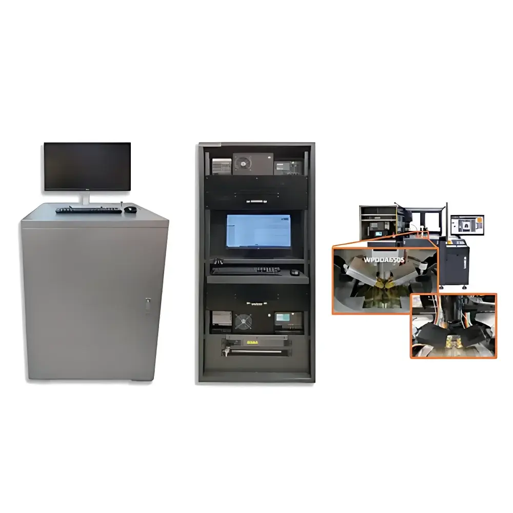
The Yingbo GaN Wafer-Level Dynamic Power Testing System is a specialized device dynamics analyzer engineered for real-time, in-situ characterization of gallium nitride (GaN) power semiconductor devices during active switching operation. Unlike conventional static parameter analyzers or general-purpose power analyzers, this system implements synchronized high-bandwidth voltage and current sampling with precisely timed gate-drive modulation to capture transient device behavior—enabling quantitative evaluation of dynamic losses, threshold voltage shift, body diode conduction, and on-resistance degradation under realistic hard-switching (HSW) and zero-voltage switching (ZVS) conditions. Its architecture supports wafer-level probing and parallel multi-DUT testing, making it suitable for both process development labs and reliability qualification workflows in compound semiconductor manufacturing.
Key Features
- Simultaneous acquisition of dynamic RDS(on), VSD, Vth, pulse I–V waveforms, and dynamic high-temperature operating life (HTOL) or stress-accelerated life test (SALT) data
- Five independently controllable acceleration parameters—temperature, drain-source voltage, gate voltage, switching frequency, and duty cycle—for MTTF modeling per JEDEC JEP180 and JESD22-A108
- Programmable gate drive with continuous –12 V to +12 V output, enabling adaptive biasing across diverse GaN HEMT gate architectures (e.g., depletion-mode vs. enhancement-mode)
- Switching frequency range from 10 kHz to 500 kHz with sub-microsecond timing resolution; minimum programmable pulse width of 1 µs
- Integrated thermal chamber support for temperature-controlled testing from 25 °C to 175 °C, compliant with MIL-STD-750 and AEC-Q101 thermal cycling requirements
- Parallel multi-DUT capability: simultaneous dynamic monitoring of up to 8 GaN dies on a single wafer using configurable probe card interfaces
- Hard-switching and soft-switching mode selection with user-defined dead-time and overlap control
Sample Compatibility & Compliance
The system accommodates standard 100 mm to 200 mm GaN-on-Si and GaN-on-SiC wafers, as well as discrete packaged devices (TO-247, PQFN, DFN). Probe interface complies with SEMI E10 and E37 standards for automated wafer probers. All measurement protocols align with industry-relevant reliability standards including JEDEC JEP180 (GaN FET dynamic characterization guidelines), JEDEC JESD22-A108 (HTOL), and IEC 60747-9 (compound semiconductor device testing). Data traceability supports GLP/GMP environments via optional audit trail logging and electronic signature modules compliant with FDA 21 CFR Part 11.
Software & Data Management
Built on a deterministic real-time Linux kernel, the embedded control software provides synchronized waveform capture, parametric extraction, and statistical trend analysis. The GUI supports scriptable test sequences (Python API), automated report generation (PDF/CSV/XLSX), and integration with LabVIEW and MATLAB via TCP/IP or shared memory. All raw oscilloscope-grade waveforms are stored with full metadata—including timestamp, environmental sensor readings, and instrument calibration status—to ensure metrological traceability. Optional cloud synchronization enables cross-site comparison of dynamic degradation trends across fabrication lots and technology nodes.
Applications
- Dynamic RDS(on) hysteresis and collapse analysis under ZVS/HWS conditions for topology-specific loss modeling
- Vth instability assessment during repetitive switching stress, correlating with trap activation energy and interface state density
- Body diode reverse recovery (VSD) characterization under high dv/dt and temperature gradients
- Pulse I–V mapping for identifying localized hot spots and current filamentation in high-current GaN HEMTs
- Accelerated dynamic reliability qualification (e.g., dynamic HTOL) aligned with AEC-Q101-012 and JEDEC JEP180 Annex B
- Wafer-level screening of dynamic parameter uniformity across die arrays to inform binning strategies
FAQ
Does the system support automatic probe alignment for wafer-level testing?
Yes—the platform integrates vision-guided auto-alignment with sub-5 µm positioning accuracy when used with compatible semi-automated probers (e.g., MPI, Cascade Microtech).
Can test data be exported in formats compatible with TCAD simulation tools?
Yes—raw waveforms and extracted parameters are exportable in SPICE-compatible .raw format and JSON schema for direct ingestion into Silvaco Atlas, Synopsys Sentaurus, or COMSOL Multiphysics.
Is calibration traceable to national metrology institutes?
All voltage, current, and temperature channels are factory-calibrated against NIST-traceable references; annual recalibration services include ISO/IEC 17025-compliant certificates.
What safety protections are implemented during high-frequency, high-voltage dynamic testing?
The system features hardware-enforced overvoltage (OVP), overcurrent (OCP), overtemperature (OTP), and arc detection with <100 ns response time, meeting IEC 61010-1 CAT II 1000 V safety requirements.


 Crystal")

 System with Parabolic Mirror Collection and Free-Space/Fiber Optical Injection")