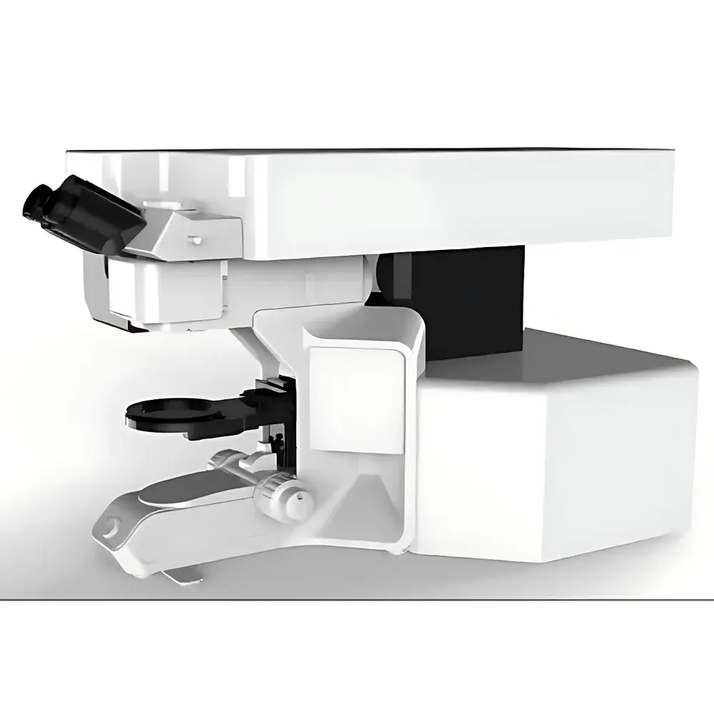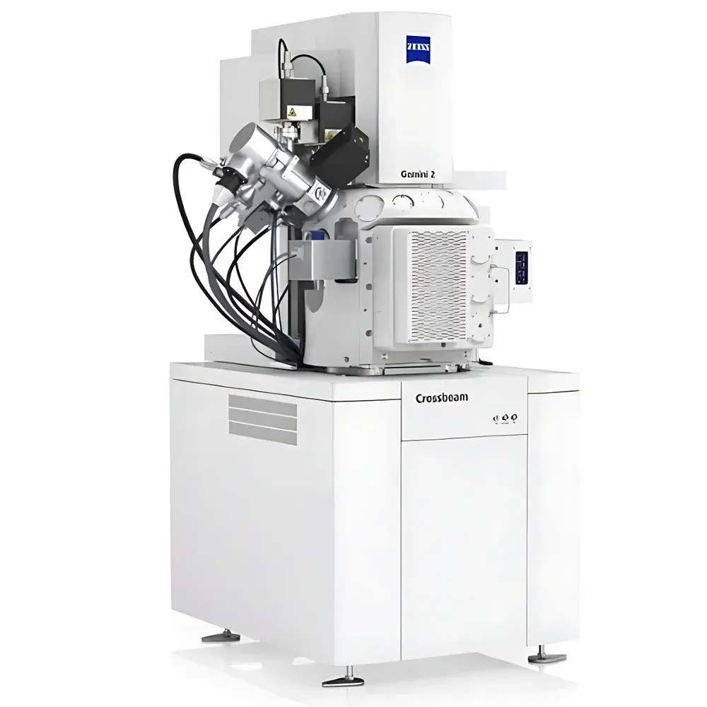
ZEISS Crossbeam Field-Emission Dual-Beam Focused Ion Beam Scanning Electron Microscope
| Brand | ZEISS |
|---|---|
| Origin | Shanghai, China |
| Manufacturer Type | Original Equipment Manufacturer (OEM) |
| Country of Origin | China |
| Model | Crossbeam |
| Instrument Type | Floor-Standing Dual-Beam System |
| Electron Source | Thermal Field-Emission Gun (TFEG) |
| Ion Source | Liquid Metal Gallium (Ga⁺) Focused Ion Beam (FIB) |
| Optional Add-on | Femtosecond Laser Ablation Module |
Overview
The ZEISS Crossbeam is a high-precision, floor-standing dual-beam focused ion beam scanning electron microscope (FIB-SEM) engineered for advanced materials characterization and site-specific sample preparation in industrial and applied research environments. Combining a thermal field-emission scanning electron microscope (SEM) with a gallium liquid metal ion source (LMIS) FIB column, the system enables simultaneous high-resolution imaging, nanoscale milling, deposition, and cross-sectional analysis. Its integrated IonSculptor™ FIB column delivers exceptional low-voltage ion beam performance—critical for minimizing ion-induced damage during TEM lamella preparation from beam-sensitive or brittle materials such as polymers, ceramics, battery electrodes, and semiconductor heterostructures. The Crossbeam serves as a complete workflow platform for preparing electron-transparent thin sections (<100 nm thickness) suitable for subsequent transmission electron microscopy (TEM) or scanning transmission electron microscopy (STEM) analysis—enabling correlative structural, compositional, and crystallographic investigation at atomic-scale resolution.
Key Features
- Thermal field-emission electron gun (TFEG) delivering high-brightness, stable electron beam for sub-nanometer SEM imaging resolution and high signal-to-noise ratio backscattered electron (BSE) and secondary electron (SE) detection.
- Gallium-based FIB column with variable acceleration voltage (typically 5–30 kV) and beam current ranging from pA to nA, optimized for both coarse milling and fine polishing with minimal curtaining and amorphization.
- Integrated end-point detection software that monitors electron yield and ion-induced secondary electron contrast changes in real time to determine lamella thickness with ±5 nm accuracy—essential for reproducible TEM-ready specimen fabrication.
- Automated, scriptable workflows for serial sectioning, lamella lift-out, and tilt-series acquisition—reducing operator dependency and improving inter-lab reproducibility.
- Optional femtosecond laser ablation module enabling rapid, non-thermal material removal for bulk sample thinning, large-area trenching, and subsurface structure exposure without FIB-induced redeposition or heat-affected zones.
- Robust mechanical design with active vibration isolation and temperature-stabilized chamber—ensuring long-term stability during multi-hour automated FIB milling or tomographic acquisitions.
Sample Compatibility & Compliance
The ZEISS Crossbeam accommodates a broad range of industrial samples—including wafers up to 300 mm diameter, packaged ICs, turbine blade coatings, composite laminates, and geological cores—via motorized stage with 100 mm × 100 mm travel and ±90° tilt capability. All vacuum and beam control subsystems comply with IEC 61000-6-3 (EMC) and IEC 61000-6-4 standards. Software architecture supports audit trail functionality aligned with GLP and GMP requirements; optional 21 CFR Part 11-compliant electronic signature and data integrity modules are available for regulated industries (e.g., medical device, pharmaceutical, and aerospace QA/QC labs). Sample preparation protocols adhere to ASTM E2782 (Standard Guide for FIB Sample Preparation) and ISO/IEC 17025:2017 documentation practices.
Software & Data Management
Operation is managed through ZEISS SMART-EM software—a unified interface for SEM/FIB alignment, pattern-based milling, automated lamella preparation, and 3D reconstruction. The platform supports DICOM-compatible export for tomographic datasets and integrates with third-party tools including Avizo, Thermo Scientific Velox, and DigitalMicrograph via open API. Raw image and log files are stored in vendor-neutral formats (e.g., TIFF, HDF5), with metadata embedded per MIAME/MINSEQ guidelines. Local storage utilizes RAID-5 configured SSD arrays; optional cloud-synced archive solutions enable secure, version-controlled collaboration across geographically distributed R&D teams.
Applications
- Localized cross-sectioning of failure sites—such as thin-film delamination, corrosion pits, embedded particulates, or interfacial voids—in microelectronics, photovoltaics, and MEMS devices.
- High-yield, parallel TEM lamella preparation from site-specific regions of interest (ROIs), including grain boundaries, phase precipitates, and dislocation networks.
- High-resolution STEM tomography of nanostructured catalysts, solid-state electrolytes, and metallurgical interfaces using tilt-series acquisition and iterative reconstruction algorithms.
- 3D nanotomography of porous media, additive-manufactured lattice structures, and biological mineralized tissues via sequential FIB milling and SEM imaging.
- Directed material removal for prototyping microfluidic channels, MEMS actuators, and plasmonic nanostructures—leveraging both FIB precision and femtosecond laser throughput.
FAQ
What electron source does the Crossbeam use, and why is it advantageous for industrial applications?
The system employs a thermal field-emission gun (TFEG), offering superior beam coherence, extended source lifetime (>2,000 hours), and stable probe current over extended imaging/milling sessions—critical for unattended operation in production-integrated metrology labs.
Can the Crossbeam prepare TEM lamellae from beam-sensitive organic or polymer samples?
Yes—low-kV FIB milling (<10 kV) combined with cryo-stage compatibility (optional) minimizes ion-induced damage and charging, enabling successful lamella extraction from soft matter, biological composites, and lithium-ion battery cathode materials.
Is the femtosecond laser module compatible with standard vacuum chamber configurations?
Yes—the laser is fiber-coupled and integrated via a dedicated optical port, requiring no modification to the main vacuum envelope; it operates synchronously with FIB/SEM acquisition under full software control.
Does the system support automated batch processing of multiple TEM lamellae?
Yes—SMART-EM includes batch scripting capabilities for multi-site lamella preparation, including auto-alignment, thickness monitoring, and lift-out sequence execution across predefined coordinates.
How is data integrity ensured during long-duration FIB-SEM tomography experiments?
All acquired images, stage positions, beam parameters, and timestamps are logged in encrypted, time-stamped HDF5 containers with SHA-256 checksums; optional 21 CFR Part 11 compliance ensures traceability for regulatory submissions.