Zhengye Aisida XG5000 Series BGA Solder Joint X-ray Inspection System
| Brand | Zhengye |
|---|---|
| Origin | Guangdong, China |
| Manufacturer Type | OEM Manufacturer |
| Regional Classification | Domestic (China) |
| Model | Aisida XG5000 Series |
| Price Range | USD 28,000 – 70,000 |
Overview
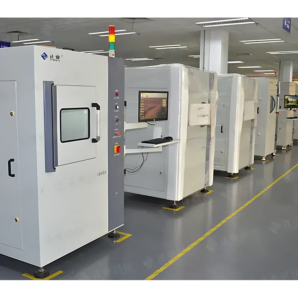
The Zhengye Aisida XG5000 Series BGA Solder Joint X-ray Inspection System is a high-resolution, real-time digital radiographic inspection platform engineered for non-destructive evaluation of microelectronic interconnects—particularly ball grid array (BGA), chip-scale package (CSP), and flip-chip solder joints. Utilizing sealed-tube microfocus X-ray generation (typically 90–130 kV, <5 µm focal spot size) and high-dynamic-range flat-panel detector technology, the system captures high-contrast transmission images based on differential X-ray attenuation across material densities and thicknesses. Designed for integration into QC/QA laboratories and production-line inline or offline inspection stations, it supports failure analysis (FA), process validation, and incoming material screening in lithium-ion battery modules, power electronics, automotive ECUs, and advanced packaging facilities.
Key Features
- 2.5D Metrology Engine: Performs calibrated geometric measurements—including linear distance, circle diameter, concentricity of multiple solder balls, and point-to-center offset—with sub-pixel spatial resolution and traceable calibration using NIST-traceable step gauges.
- CNC Path Programming: Enables repeatable, operator-independent inspection routines via teach-mode path recording; stores up to 256 programmable coordinate sets with motorized XYZ stage control (±0.5 µm repeatability) and Z-axis focus compensation.
- Intelligent Navigation Interface: Features a dual-display architecture: a large-format overview map (1024 × 768 px) synchronized with real-time magnified ROI view; click-to-navigate functionality reduces manual stage adjustment time by >70% during multi-site inspection.
- Real-Time Image Processing Pipeline: Supports live histogram equalization, edge enhancement (Sobel/LoG filters), noise suppression (adaptive median filtering), contrast stretching, and dynamic range compression—all applied pre-acquisition without latency penalty.
- Digital Detector Architecture: Equipped with a 14-bit, 2048 × 2048 pixel amorphous silicon flat-panel detector (pixel pitch: 100 µm), delivering >65 dB dynamic range and <1.5% non-uniformity across full field-of-view.
Sample Compatibility & Compliance
The XG5000 accommodates PCB assemblies up to 400 × 300 mm (L × W) and 50 mm max height, including populated automotive control units, cylindrical/prismatic battery cells (with optional rotating fixture), and stacked SiP modules. It complies with IEC 61340-5-1 (ESD protection), IEC 62471 (LED/X-ray optical radiation safety), and meets Class II radiation safety requirements per CNCA-C11-01:2020. All software workflows support audit trail logging aligned with ISO/IEC 17025 documentation requirements and are compatible with GLP/GMP environments when configured with user access control and electronic signature modules.
Software & Data Management
The proprietary Aisida VisionInsight™ software (v4.2+) provides fully automated pass/fail classification based on user-defined defect templates—such as voiding >25% cross-sectional area, bridging between adjacent solder balls, or missing solder joints. Measurement data exports directly to CSV, XML, or PDF reports with embedded annotated images and timestamped metadata. Integrated DICOM export enables PACS interoperability for cross-departmental FA collaboration. Software validation documentation (IQ/OQ/PQ protocols) and 21 CFR Part 11-compliant electronic record packages are available upon request for regulated manufacturing sites.
Applications
- Void quantification and distribution mapping in SnAgCu solder joints under BGA components
- Interfacial delamination detection at copper pad–solder interface in high-power modules
- Electrode tab weld integrity verification in prismatic Li-ion battery cells
- Conformal coating thickness uniformity assessment via dual-energy subtraction mode
- Post-reflow solder joint coalescence validation in high-density HDI PCBs
- Counterfeit component identification through internal die structure and wire bonding topology analysis
FAQ
What is the minimum detectable void size in a 0.3-mm-diameter solder ball?
Under standard acquisition conditions (120 kV, 0.8 µA, 1.2 s exposure), the system resolves voids ≥15 µm in diameter with >95% detection probability (per ASTM E2737-21 Annex A1).
Does the system support automated reporting compliant with IPC-A-610 or J-STD-001?
Yes—preconfigured report templates include IPC-A-610 Class 2/3 defect taxonomy, solder joint acceptance criteria, and measurement uncertainty annotations per GUM (JCGM 100:2008).
Can the XG5000 be integrated into a factory MES or SPC system?
Via OPC UA (v1.04) and RESTful API interfaces, raw image metadata, measurement logs, and pass/fail status can be streamed to Siemens Opcenter, Rockwell FactoryTalk, or custom SQL-based SPC dashboards.
Is radiation shielding built-in or required externally?
The cabinet is certified as a fully shielded Class II X-ray enclosure (lead-equivalent thickness ≥2.0 mm Pb), requiring no additional room shielding for operation at rated tube voltage and current.
What calibration standards are supplied with the system?
NIST-traceable tungsten step wedge (0.1–5.0 mm Al eq.), stainless steel pin gauge set (10–500 µm), and Cu sphere phantom (Ø50 µm–1.0 mm) for daily performance verification and annual metrological recalibration.


