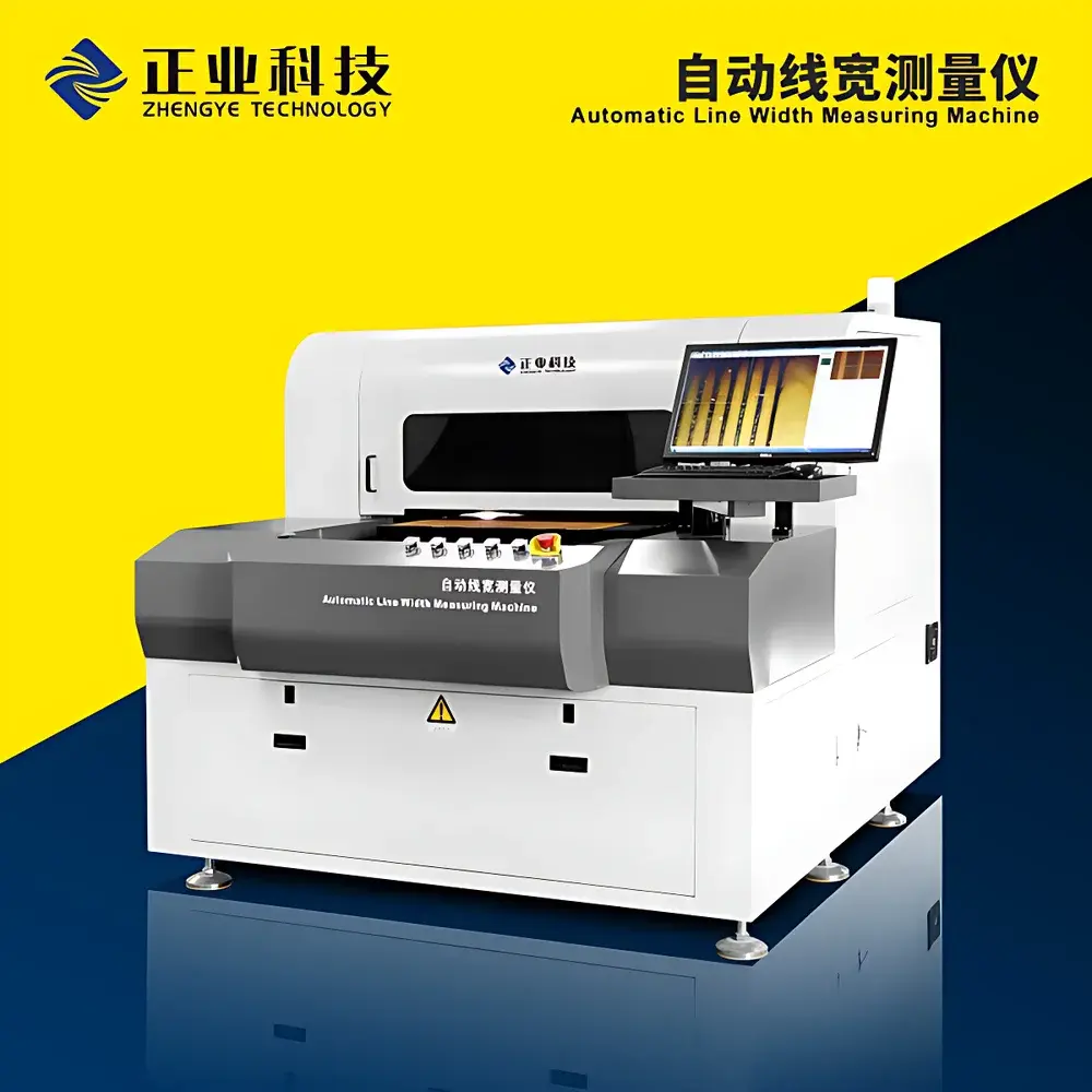
Zhengye ASIDA32 Automated PCB Line Width and Spacing Measurement System
| Brand | Zhengye |
|---|---|
| Origin | Guangdong, China |
| Manufacturer Type | OEM/ODM Manufacturer |
| Region Classification | Domestic (China) |
| Model | ASIDA32 |
| Pricing | Available Upon Request |
Overview
The Zhengye ASIDA32 Automated PCB Line Width and Spacing Measurement System is a high-precision optical metrology instrument engineered for non-contact, quantitative inspection of critical dimensional features on printed circuit boards (PCBs) and related microelectronic substrates. It operates on the principle of digital image acquisition combined with sub-pixel edge detection algorithms, enabling traceable, repeatable measurement of line widths, line-to-line spacing, pad-to-trace distances, hole-to-edge clearances, circular via diameters, blind via profiles, and arc radii. Designed for use post-etching—prior to solder mask application—the system supports both inner-layer and outer-layer copper pattern verification. Its optical architecture integrates a fixed-magnification telecentric lens, high-resolution monochrome CMOS sensor, and coaxial red LED illumination for consistent contrast enhancement and low-parallax imaging. The ASIDA32 complies with industry-standard geometric dimensioning requirements defined in IPC-6012, IPC-A-600, and IPC-TM-650 Section 2.2.15, ensuring alignment with global PCB fabrication quality control protocols.
Key Features
- Precision optical measurement platform with motorized Z-axis focus adjustment for optimal depth-of-field control across varying copper thicknesses and surface topographies.
- Sub-pixel edge localization algorithm (≤0.1 pixel resolution) for accurate determination of conductor boundaries under variable lighting and etch profile conditions.
- Red LED coaxial illumination system providing uniform, glare-free contrast for reliable edge extraction on matte, semi-gloss, or oxidized copper surfaces.
- Automated feature recognition engine capable of detecting and classifying lines, gaps, pads, vias (through-hole and blind), arcs, and irregular contours without manual ROI definition.
- Integrated SPC module compliant with ISO 7870-2 and ASTM E2587 standards, supporting real-time control charting (X-bar/R, Cpk/Ppk), trend analysis, and export of statistical summaries in CSV and PDF formats.
- Modular software architecture supporting user-defined measurement templates, multi-point batch sequencing, and pass/fail logic based on configurable tolerance bands per feature type.
Sample Compatibility & Compliance
The ASIDA32 accommodates standard PCB panel sizes up to 610 mm × 457 mm (24″ × 18″) with optional stage extensions for larger formats. It supports rigid FR-4, flexible polyimide (PI), and rigid-flex hybrid substrates, as well as silicon wafers, thin-film transistor (TFT) glass panels, and IC die surfaces. All measurements are traceable to NIST-calibrated reference standards through documented calibration procedures aligned with ISO/IEC 17025 requirements. The system meets electromagnetic compatibility (EMC) directives per GB/T 18268.1–2010 (equivalent to IEC 61326-1) and safety standards per GB 4793.1–2007 (IEC 61010-1). Data integrity safeguards include audit trail logging, electronic signature support, and user role-based access control—facilitating compliance with GLP, GMP, and internal QA documentation policies.
Software & Data Management
The ASIDA32 runs on a Windows-based metrology suite featuring a dual-mode interface: guided wizard mode for routine operators and advanced scripting mode (via Lua API) for integration into factory MES or AOI data pipelines. Raw images, coordinate metadata, measurement logs, and SPC reports are stored in an encrypted SQLite database with automatic daily backup and versioned archiving. Export options include XML (for IPC-2581 interoperability), JSON (for RESTful API ingestion), and standardized Excel-compatible .xlsx files. Software validation documentation—including IQ/OQ protocols and change control records—is available upon request to support regulated environment deployments.
Applications
- Final verification of etch uniformity and line width variation (CD uniformity) across PCB production lots.
- Process capability assessment for fine-pitch routing (e.g., ≤50 µm lines/spaces) in HDI and RF multilayer boards.
- Root cause analysis of undercut/over-etch defects by comparing upper vs. lower line width profiles.
- Qualification of laser direct imaging (LDI) systems through correlation of measured features against photoplotter Gerber data.
- Inline metrology support for automated optical inspection (AOI) system calibration and reference standard generation.
- Cross-functional use in semiconductor packaging substrates, touch panel ITO patterning, and MEMS device lithography monitoring.
FAQ
What is the minimum measurable line width supported by the ASIDA32?
The practical resolution limit depends on optical magnification and pixel pitch; typical configurations achieve reliable measurement down to 15–20 µm line widths under optimal contrast and focus conditions.
Does the system support measurement of non-vertical sidewall profiles (e.g., trapezoidal etch profiles)?
Yes—the dual-edge detection algorithm captures independent upper and lower boundary coordinates, enabling calculation of sidewall angle and etch bias when used with calibrated focus stacking routines.
Can measurement data be integrated into a centralized SPC server or ERP system?
Yes—via TCP/IP socket communication, OPC UA connectivity, or scheduled file export using configurable naming conventions and directory paths.
Is the software validated for use in FDA-regulated environments?
While the base software is not pre-certified for 21 CFR Part 11, it includes all technical prerequisites (audit trails, electronic signatures, role-based permissions); full validation support packages—including test scripts and UAT documentation—are available under NDA.
What maintenance is required to ensure long-term measurement stability?
Annual recalibration using certified step gauges and contrast targets is recommended; routine cleaning of optics and verification of illumination intensity drift should be performed per the preventive maintenance schedule in the operator manual.