Zhengye XK32A Automated PCB Line Width & Spacing Measurement System
| Brand | Zhengye |
|---|---|
| Origin | Guangdong, China |
| Manufacturer Type | OEM/ODM Manufacturer |
| Country of Origin | China |
| Model | XK32A |
| Pricing | Available Upon Request |
Overview
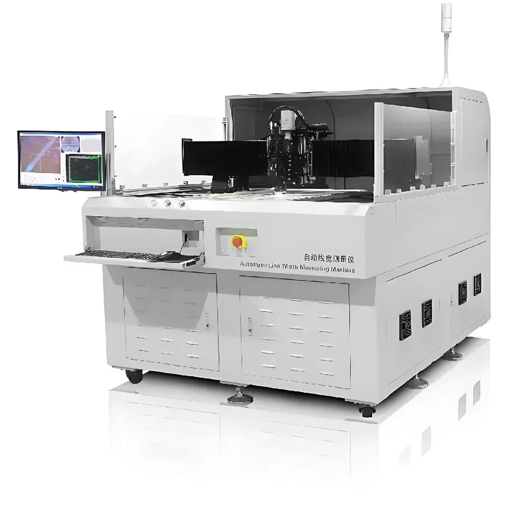
The Zhengye XK32A Automated PCB Line Width & Spacing Measurement System is an industrial-grade optical metrology platform engineered for non-contact, high-precision dimensional analysis of printed circuit board (PCB) features. It operates on the principle of digital image acquisition and sub-pixel edge detection: a high-resolution monochrome CMOS camera captures orthogonally illuminated top-down images of PCB substrates—typically after etching and prior to solder mask application. Integrated illumination modules provide uniform, glare-free backlighting and coaxial surface lighting to enhance contrast across copper traces, pads, and drill holes within the field of view. The system delivers quantitative measurements of line width (top and bottom profiles), line spacing, circular hole diameter, and gold finger width—critical parameters defined in IPC-6012, IPC-A-600, and IPC-TM-650 test methods. Designed for inline or offline deployment in Class 10K cleanroom environments, the XK32A supports traceable measurement workflows compliant with ISO/IEC 17025 requirements for calibration and uncertainty estimation.
Key Features
- Fourth-generation optical architecture featuring 5-megapixel progressive-scan CMOS sensor with 2.2 µm pixel pitch and hardware-triggered exposure control
- Dual-illumination mode: adjustable coaxial LED ring light for surface feature contrast + independent transmitted LED backlight for through-hole and substrate edge definition
- Real-time image capture at ≥15 fps with onboard FPGA-based preprocessing (noise reduction, histogram equalization, adaptive thresholding)
- Sub-pixel edge localization algorithm achieving ≤0.5 µm repeatability in line width measurement under controlled lab conditions
- Motorized Z-axis focus adjustment with closed-loop stepper control and auto-focus validation via sharpness metric feedback
- Rugged aluminum-alloy frame with anti-vibration damping mounts; designed for continuous operation in factory-floor environments (IP54-rated enclosure optional)
Sample Compatibility & Compliance
The XK32A accommodates standard rigid PCBs up to 610 mm × 457 mm (24″ × 18″) and thicknesses from 0.05 mm to 3.2 mm. Flexible and rigid-flex boards may be measured using vacuum-assisted flatness stabilization fixtures (sold separately). All measurement outputs include timestamped metadata, operator ID, job lot number, and instrument calibration status—enabling full audit trail generation per FDA 21 CFR Part 11 and GLP/GMP documentation standards. Software-generated reports conform to IPC-D-322 template structure and support export in PDF/A-1b, CSV, and XML formats for MES integration. System validation documentation includes IQ/OQ protocols aligned with ISO 9001:2015 clause 7.1.5 and ASTM E2919-20 guidelines for optical measurement systems.
Software & Data Management
The proprietary Zhengye VisionMetro v4.2 software suite runs on Windows 10 IoT Enterprise (64-bit) and provides intuitive workflow-driven measurement sequencing. Users define multi-point inspection plans via graphical overlay on reference templates; measurement zones can be saved as reusable “recipe files” with configurable tolerance bands (±X µm absolute or ±Y% relative). The software incorporates statistical process control (SPC) modules supporting X-bar/R charts, Cp/Cpk calculation, and real-time SPC alarm triggers. All raw images and processed data are stored in AES-256 encrypted local SQLite databases with optional network backup to secure NAS endpoints. Audit logs record every user action—including parameter edits, pass/fail overrides, and calibration interventions—with SHA-256 hashing for integrity verification.
Applications
- Pre-solder mask verification of inner/outer layer etch quality in HDI, mSAP, and 5G mmWave RF multilayer boards
- Statistical sampling of line width uniformity across panelized arrays for process capability studies
- Root cause analysis of undercut/over-etch defects via comparative top-bottom profile asymmetry quantification
- Qualification testing of new etchant chemistries or exposure dose parameters in R&D labs
- Supplier incoming inspection per IPC-A-600 acceptance criteria for conductor geometry
- Supporting IPC-2221B design rule verification during NPI (New Product Introduction) stages
FAQ
What is the minimum measurable line width supported by the XK32A?
The system achieves reliable detection of features ≥15 µm under optimal contrast conditions; recommended minimum nominal line width is 25 µm for routine production use.
Does the system support automatic defect classification (e.g., bridging, open circuit)?
Yes—VisionMetro v4.2 includes configurable rule-based defect recognition engines trained on IPC-defined anomaly categories, with user-definable severity thresholds.
Is calibration traceable to national metrology institutes?
Yes—optional NIST-traceable calibration kits (line width standards, step height gauges) are available with certificate of calibration valid for 12 months.
Can the XK32A integrate with factory MES or ERP systems?
Yes—via RESTful API interface supporting JSON payloads; pre-built connectors exist for Siemens Opcenter, Rockwell FactoryTalk, and Mitsubishi MELSEC platforms.
What maintenance schedule is recommended for long-term accuracy stability?
Daily visual inspection of optics and lighting; quarterly verification using certified reference standards; annual full system recalibration including camera lens MTF characterization and illumination uniformity mapping.


