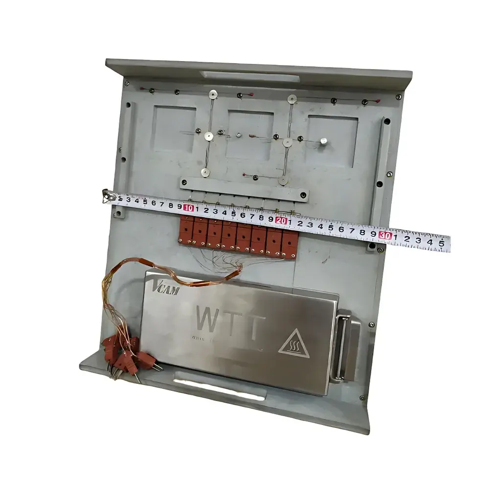

Zhengye XK32A Fully Automated PCB Line Width Measurement System
| Brand | Zhengye |
|---|---|
| Origin | Guangdong, China |
| Manufacturer Type | OEM/ODM Manufacturer |
| Regional Classification | Domestic (China) |
| Model | XK32A |
| Pricing | Upon Request |
Overview
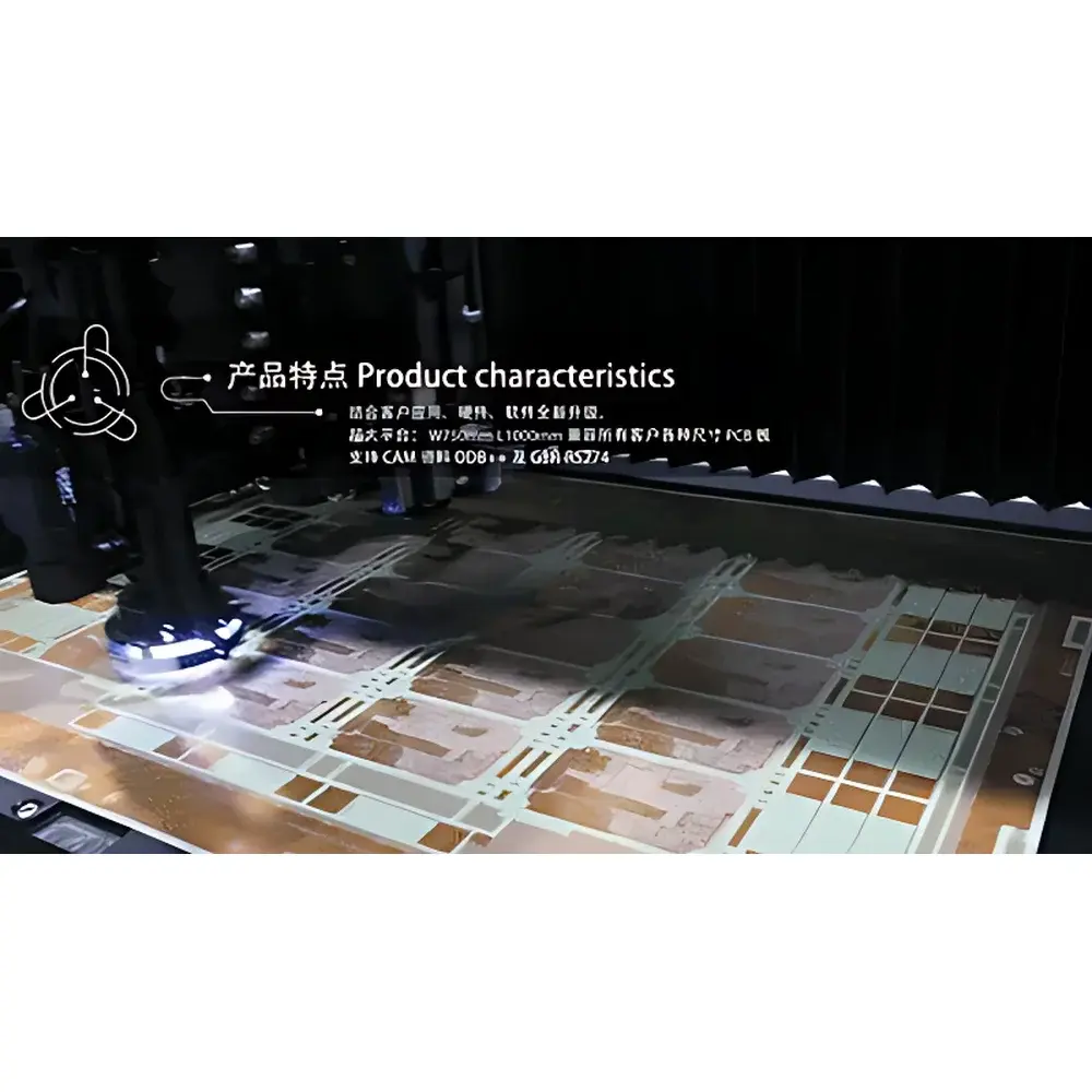
The Zhengye XK32A Fully Automated PCB Line Width Measurement System is an optical metrology instrument engineered for high-precision, non-contact dimensional inspection of printed circuit board (PCB) features during mid-process fabrication. It operates on the principle of high-resolution digital imaging combined with calibrated machine vision algorithms to quantify critical geometric parameters—including line width (top and bottom), line spacing (pitch), circular via diameters, and gold finger trace widths—on both inner and outer layer panels after developing and etching, but prior to solder mask application. Designed specifically for 5G-capable HDI and standard FR-4 substrates, the system delivers repeatable sub-micron measurement capability within its field of view, supporting process control in ISO 9001- and IPC-A-600-compliant manufacturing environments.
Key Features
- Fourth-generation optical architecture featuring coaxial LED illumination and telecentric lensing to minimize perspective distortion and ensure consistent edge contrast across varying copper thicknesses and surface finishes.
- Real-time image acquisition via industrial-grade CMOS camera with adjustable exposure and white balance, synchronized to stage motion for seamless multi-field stitching.
- Automated XY motorized stage with programmable positioning accuracy of ±1 µm, enabling full-panel scanning or targeted ROI (region-of-interest) inspection based on Gerber file alignment.
- Embedded measurement engine compliant with IPC-TM-650 2.2.17 (Optical Dimensional Measurement) methodology, supporting configurable tolerance bands per feature type and layer.
- Robust mechanical design with vibration-dampened base and thermal-stabilized enclosure, ensuring long-term calibration stability under continuous factory-floor operation.
Sample Compatibility & Compliance
The XK32A accommodates rigid, flex, and rigid-flex PCBs up to 610 mm × 610 mm (24″ × 24″), with thickness ranging from 0.05 mm to 3.2 mm. It supports both bare copper and tin-lead/tin-silver surface finishes without requiring conductive coating or vacuum fixation. Measurement outputs are traceable to NIST-traceable standards through annual calibration protocols documented per ISO/IEC 17025 requirements. The system meets IPC-A-600G Class 2 and Class 3 acceptance criteria for conductor geometry verification and generates audit-ready reports aligned with internal quality management systems (QMS) and customer-facing PPAP documentation.
Software & Data Management
The proprietary Zhengye VisionInsight™ software provides a Windows-based GUI with dual-mode operation: manual measurement for R&D validation and fully automated batch mode for inline SPC (Statistical Process Control). All measurements include timestamped metadata, operator ID, job number, and image capture logs. Raw images and coordinate data are stored in lossless TIFF format; summary results export to CSV, XLSX, or PDF with embedded pass/fail flags. Audit trail functionality records user actions, parameter changes, and calibration events—supporting GLP/GMP-aligned environments where 21 CFR Part 11 electronic signature readiness can be enabled via optional configuration.
Applications
- Post-etch verification of fine-line circuits (≤50 µm line/space) in 5G RF modules and high-speed digital interconnects.
- Process capability analysis (Cp/Cpk) for electroplating and pattern transfer steps across multiple production lots.
- Root cause investigation of undercutting, over-etching, or photoresist slivering via comparative cross-sectional profile overlays.
- Supplier qualification support by generating standardized measurement reports accepted by Tier-1 automotive and aerospace electronics OEMs.
- Integration into Industry 4.0 infrastructure via OPC UA interface for MES connectivity and real-time dashboarding of yield KPIs.
FAQ
What is the minimum measurable line width supported by the XK32A?
The system achieves reliable detection down to 25 µm line width under optimal lighting and contrast conditions, subject to substrate surface roughness and copper grain structure.
Does the system require physical contact with the PCB during measurement?
No—measurements are fully non-contact and optical; no probe loading, vacuum chucking, or surface preparation is needed.
Can the XK32A integrate with existing factory automation systems?
Yes, it supports RS-232, Ethernet/IP, and optional OPC UA communication protocols for bidirectional data exchange with MES and SCADA platforms.
Is software validation documentation available for regulated industries?
Comprehensive IQ/OQ documentation packages—including test scripts, evidence logs, and URS mapping—are provided upon request for pharmaceutical or medical device PCB suppliers adhering to ISO 13485.
How frequently does the system require recalibration?
Annual calibration is recommended; however, daily verification using certified reference standards (e.g., NIST-traceable reticles) is advised as part of routine QC checks.