
ZOLIX STS Series Integrated Raman/Photoluminescence/Photoelectric Current Characterization System
| Brand | ZOLIX |
|---|---|
| Origin | Beijing, China |
| Manufacturer Type | Direct Manufacturer |
| Product Origin | Domestic (China) |
| Model | STS Series |
| Pricing | Available Upon Request |
Overview
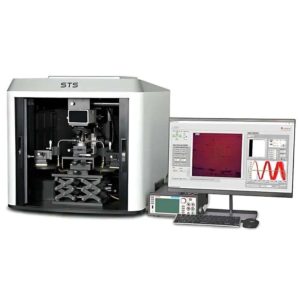
The ZOLIX STS Series Integrated Raman/Photoluminescence/Photoelectric Current Characterization System is an advanced multimodal in-situ analytical platform engineered for correlative microspectroscopic and microelectronic characterization of optoelectronic materials and devices. Built upon the modular RTS-mini confocal microscope architecture, the system enables synchronized acquisition of Raman scattering, photoluminescence (PL), time-resolved PL decay, and spatially resolved photocurrent response—all under identical optical excitation conditions and precise sample positioning. Its core measurement principles include confocal Raman spectroscopy (based on inelastic photon-phonon scattering), time-correlated single-photon counting (TCSPC) for nanosecond-to-microsecond fluorescence lifetime imaging, and precision current-voltage (I-V) metrology via integrated source-measure units (SMUs). This tri-modal capability supports fundamental investigation of molecular vibrational and rotational energy structures, carrier generation–recombination kinetics, local absorption efficiency, charge separation dynamics at heterojunctions, and spatial heterogeneity in semiconductor interfaces—critical for R&D in perovskite solar cells, 2D materials, quantum dots, organic photodetectors, and thin-film transistors.
Key Features
- Triple-modality integration: Simultaneous or sequential Raman spectroscopy, steady-state & time-resolved photoluminescence imaging, and microscale photocurrent mapping within a single optical path.
- High-resolution confocal optics: Fiber-coupled confocal design with diffraction-limited spatial resolution ≤1 μm (at 100×, NA 0.9 objective, 532 nm excitation).
- Extended spectral coverage: Raman shift range 60–6000 cm⁻¹ (with 532 nm laser); UV–NIR photoluminescence detection from 200–900 nm; full CCD spectral response 200–1100 nm.
- Ultrafast lifetime detection: TCSPC-based fluorescence lifetime imaging with minimum time resolution of 16 ps and measurable decay range from 500 ps to 10 μs.
- Precision microelectronic probing: Integrated Keithley 2450 SourceMeter® with current measurement range 1 nA–1 A, 20 fA resolution, <50 pA dark noise, and 0.03% basic accuracy.
- Automated micro-positioning: High-stability motorized XYZ stage (5 μm positional resolution) combined with independent probe-stage translation (0.7 μm resolution) and vacuum chuck (65 mm diameter) for repeatable device contact alignment.
Sample Compatibility & Compliance
The STS system accommodates standard semiconductor wafers (Si, GaAs, perovskites), thin-film devices (OPVs, OLEDs), 2D material flakes (MoS₂, WSe₂), and micro-patterned electrodes on glass or silicon substrates. Sample mounting is compatible with ambient, inert-gas glovebox, and low-vacuum environments (optional chamber integration). All electrical measurements comply with IEC 61000-4-8 (conducted immunity) and meet functional safety requirements for Class I laboratory equipment. Data acquisition protocols support audit-ready traceability per GLP and GMP frameworks; optional software modules enable 21 CFR Part 11-compliant electronic signatures and secure user access control.
Software & Data Management
Control and analysis are unified through ZOLIX’s proprietary STS Control Suite—a Windows-based application supporting real-time hardware synchronization, multi-channel data fusion, and batch processing workflows. The software provides native support for Raman peak fitting (Lorentzian/Gaussian deconvolution), PL lifetime decay modeling (multi-exponential fitting), LBIC (laser-beam-induced current) image quantification, and pixel-wise I-V curve extraction. Export formats include HDF5 (for FAIR data compliance), ASCII, and industry-standard .csv/.tiff. Raw spectral and temporal datasets are timestamped and metadata-tagged (laser power, integration time, objective ID, environmental temperature), ensuring reproducibility across labs and longitudinal studies.
Applications
- Correlative defect mapping in halide perovskite films: linking local Raman mode broadening, non-radiative recombination lifetimes, and photocurrent quenching zones.
- Interface quality assessment in organic–inorganic hybrid photovoltaics: quantifying charge transfer efficiency at donor–acceptor junctions via spatially registered PL quenching and photocurrent onset maps.
- Strain and doping profiling in transition metal dichalcogenides: combining Raman E²g/A₁g peak shifts, PL peak energy shifts, and local series resistance derived from I-V mapping.
- Reliability testing of flexible photodetectors: in-situ monitoring of degradation-induced changes in Raman crystallinity, PL quantum yield, and photoconductive gain under bias stress.
- Fundamental carrier dynamics in quantum-confined nanostructures: extracting exciton binding energy (from PL peak position vs. temperature), phonon coupling strength (via Raman linewidth), and hot-carrier extraction efficiency (from transient photocurrent rise time).
FAQ
Can the system perform simultaneous Raman and photocurrent acquisition?
Yes—the optical path is shared across all modalities, and hardware triggering allows synchronized data capture with sub-millisecond timing alignment between spectroscopic and electrical channels.
Is vacuum or cryogenic operation supported?
The base configuration operates under ambient conditions; optional cryostat and vacuum chamber adapters are available for low-temperature (4–300 K) and controlled-atmosphere measurements.
What laser options are available beyond the standard 532 nm source?
Configurable excitation sources include 405 nm (for UV-Raman and lifetime imaging), 638 nm (for reduced photodegradation in organics), and dual-wavelength setups enabling pump–probe photocurrent contrast analysis.
How is electrical contact established during LBIC mapping?
Tungsten probe tips (5/10/20 μm diameter) are mounted on precision XYZ manipulators; contact force is manually optimized prior to scanning, and probe wear is monitored via real-time resistance feedback.
Does the software support automated batch processing for large-area mapping datasets?
Yes—scriptable analysis pipelines enable unattended processing of >10⁴-pixel hyperspectral maps, including background subtraction, spectral normalization, lifetime histogram generation, and overlay rendering of Raman/PL/photocurrent parameter maps.


")
