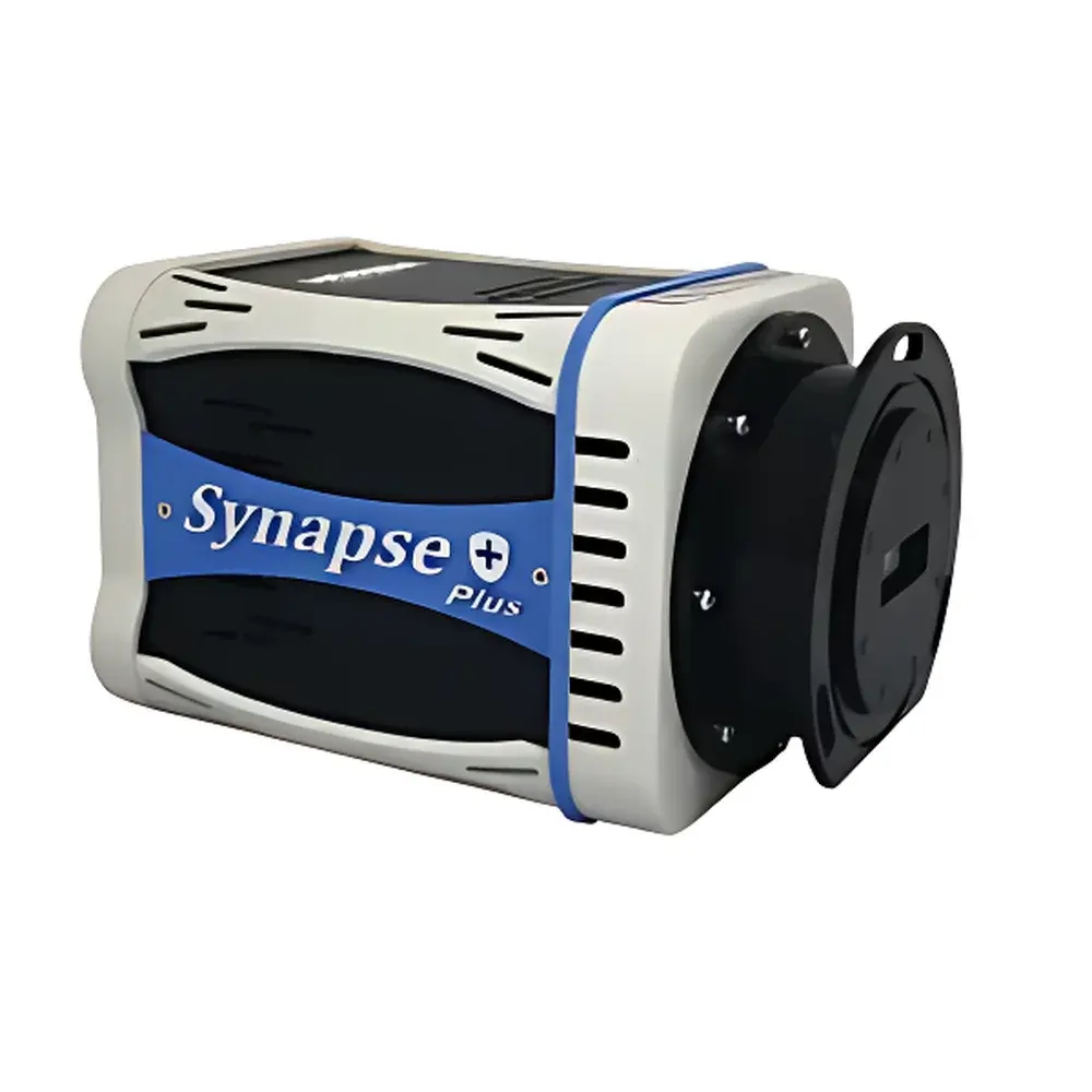
HORIBA Synapse Plus High-Speed CCD Detector
| Brand | HORIBA |
|---|---|
| Origin | USA |
| Manufacturer Type | Manufacturer |
| Origin Category | Imported |
| Model | Synapse Plus High-Speed CCD |
| Pricing | Upon Request |
Overview
The HORIBA Synapse Plus High-Speed CCD Detector is a thermoelectrically cooled, scientific-grade imaging sensor engineered for high-fidelity spectral acquisition across the ultraviolet to near-infrared (UV–NIR) range (200–1100 nm). Built upon back-illuminated and front-illuminated CCD architectures, it delivers exceptional quantum efficiency, low dark current, and high dynamic range—critical attributes for demanding applications in Raman spectroscopy, photoluminescence mapping, time-resolved emission studies, and process analytical technology (PAT). Unlike liquid-nitrogen-cooled alternatives, the Synapse Plus employs a robust two-stage TE cooling system capable of stabilizing the sensor at –75 °C (standard) or –95 °C (with optional external chiller), enabling long-exposure, low-noise acquisitions without cryogenic infrastructure. Its vacuum-sealed, single-window housing ensures permanent hermeticity and eliminates condensation or outgassing risks—eliminating routine maintenance over the detector’s operational lifetime.
Key Features
- Ultra-Low Noise Architecture: A custom low-noise amplifier is integrated directly adjacent to the CCD die, minimizing signal path length and electromagnetic interference—resulting in read noise as low as 3.5 e⁻ rms (typical) at 1 MHz readout.
- High Signal Linearity: Digitally calibrated analog front-end electronics ensure >99.9% linearity across the full well capacity (up to 100,000 e⁻), validated per unit during factory testing with NIST-traceable photometric standards.
- Multi-Configuration Sensor Options: Available in FI (front-illuminated), BI (back-illuminated), and BIDD (deep-depletion back-illuminated) variants—each optimized for specific spectral bands (UV, VIS, NIR) and quantum efficiency profiles (peak QE up to 95% at 600 nm).
- Dual-Channel Synchronization: Integrated auxiliary analog input accepts voltage or current signals from PMTs, Si photodiodes, or InGaAs detectors—enabling real-time reference normalization, extended wavelength coverage beyond CCD limits, or simultaneous multi-detector acquisition.
- Programmable TTL Triggering: Dual-edge (rising/falling) programmable inputs and outputs support precise synchronization with lasers, shutters, or scanning stages—essential for pump-probe, gated detection, or multiplexed optical setups.
- Onboard Shutter Control: Integrated shutter driver circuitry enables hardware-synchronized exposure control and background subtraction—eliminating the need for external trigger modules or timing adapters.
Sample Compatibility & Compliance
The Synapse Plus is designed for integration into HORIBA’s modular spectroscopic platforms—including iHR, TriVista, and LabRAM systems—but maintains full compatibility with third-party Czerny–Turner, echelle, and flat-field spectrometers via standard 42-mm or 50-mm flange interfaces. Its sealed vacuum housing complies with IEC 61000-6-3 (EMC immunity) and meets RoHS 2011/65/EU requirements. For regulated environments, data integrity is supported through SynerJY® software’s audit trail functionality, which logs all acquisition parameters, user actions, and calibration events—aligning with GLP/GMP documentation expectations and FDA 21 CFR Part 11 electronic record principles when deployed with appropriate IT validation protocols.
Software & Data Management
Control and data acquisition are managed via HORIBA’s SynerJY® software—a Windows-based platform supporting real-time preview, multi-region-of-interest (ROI) analysis, spectral stitching, and kinetic series export in HDF5, ASCII, and vendor-neutral .spe formats. The Synapse Plus SDK provides full API access (C/C++, Python bindings) for custom automation, including pixel binning, region-specific gain adjustment, non-uniformity correction (NUC), and synchronized multi-channel acquisition. LabVIEW® VIs are certified for NI LabVIEW 2020 SP1 and later, enabling seamless integration into existing test benches governed by IEEE 1622 or ASTM E2807 digital instrumentation standards.
Applications
- Raman and resonance Raman spectroscopy of nanomaterials, pharmaceuticals, and 2D semiconductors
- Time-resolved photoluminescence decay profiling in perovskite solar cells and quantum dots
- In-line UV-Vis-NIR monitoring of chemical reactions and polymerization kinetics
- Microspectroscopy and hyperspectral imaging using fiber-coupled or microscope-integrated configurations
- Calibration transfer between reference and field instruments via intensity-stabilized reference channel
FAQ
What cooling temperature does the Synapse Plus achieve without external chillers?
The standard two-stage TE cooler reaches –75 °C; with an optional recirculating chiller, operation down to –95 °C is supported.
Is the detector compatible with non-HORIBA spectrometers?
Yes—mechanical and electrical interfaces follow industry-standard dimensions and TTL/USB 2.0 protocols; optical coupling requires appropriate f/# matching and collimation alignment.
How is dark current characterized and validated at the factory?
Each unit undergoes 30-minute dark frame acquisition at specified temperatures; dark current is calculated per pixel and reported in the certificate of conformance alongside read noise and linearity metrics.
Can the auxiliary input be used for real-time laser power monitoring during Raman acquisition?
Yes—the analog input operates synchronously with CCD exposure; users may apply real-time ratioing (e.g., sample signal / reference diode) within SynerJY® or custom scripts.
Does the Synapse Plus support hardware binning?
Yes—vertical and horizontal binning modes are configurable via software or SDK, with corresponding adjustments to effective pixel size and readout speed.


