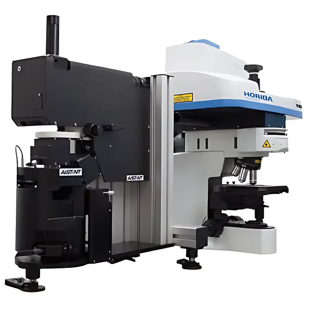

HORIBA XploRA Nano AFM-Raman Correlative Microscopy System
| Brand | HORIBA |
|---|---|
| Origin | France |
| Manufacturer Type | Original Equipment Manufacturer (OEM) |
| Import Status | Imported |
| Model | XploRA Nano |
| Instrument Type | Confocal Micro-Raman Spectrometer with Integrated Atomic Force Microscopy |
| Spectral Range | 50–9000 cm⁻¹ |
| Spectral Resolution | 1 cm⁻¹ |
| Spatial Resolution (TERS mode) | <10 nm |
| Minimum Wavenumber | 50 cm⁻¹ |
| Spectral Reproducibility | <0.1 cm⁻¹ |
Overview
The HORIBA XploRA Nano is a fully integrated AFM-Raman correlative microscopy system engineered for nanoscale chemical and physical characterization. It combines confocal micro-Raman spectroscopy—based on laser excitation and inelastically scattered photon detection—with high-resolution atomic force microscopy (AFM) in a single, co-registered platform. Unlike sequential or loosely coupled systems, the XploRA Nano employs direct optical path integration to ensure sub-10 nm spatial registration between topographic, mechanical, and vibrational spectral data. This enables true correlative analysis where Raman spectral signatures are acquired *exactly* at the same location probed by the AFM tip—critical for validating structural heterogeneity, interfacial chemistry, defect distribution, and strain mapping in 2D materials, nanotubes, polymers, and biological nanostructures. The system operates on a modular architecture compatible with multiple scanning probe modalities (AFM, STM, SNOM), supporting both far-field confocal Raman imaging and near-field tip-enhanced Raman scattering (TERS).
Key Features
- True co-localized AFM and Raman imaging: Simultaneous acquisition of topography, mechanical properties (e.g., modulus, adhesion), and position-matched Raman spectra with <10 nm spatial correlation accuracy.
- Optimized TERS implementation: Dedicated optical train with active tip-laser alignment, high-NA objective coupling (up to ×100, NA > 0.9), and vibration-isolated high-frequency AFM scanner enabling stable sub-10 nm TERS mapping.
- Triple optical coupling flexibility: Bottom illumination (for transparent substrates), top illumination (for co-located confocal Raman/AFM or tilted-tip TERS), and side illumination (for opaque or highly scattering samples).
- Automated laser alignment: Real-time photodiode-based feedback for AFM photolever laser collimation—minimizing setup drift and ensuring long-term measurement stability.
- High-throughput spectral acquisition: Back-illuminated CCD detector with deep-cooling (−70 °C), combined with optimized light collection optics, supports rapid point-by-point or line-scan Raman mapping synchronized with AFM rastering.
- Modular SPM compatibility: Designed for seamless integration with third-party AFM/STM platforms via standardized mechanical and electrical interfaces; full software control over both subsystems from a unified GUI.
Sample Compatibility & Compliance
The XploRA Nano accommodates diverse sample types—including conductive and insulating substrates, thin films, exfoliated 2D crystals, biological membranes, polymer blends, and catalytic nanoparticles—without requiring metallization or special preparation. Its wide spectral range (50–9000 cm⁻¹) supports low-frequency phonon modes (e.g., interlayer shear modes in graphene), mid-range functional group vibrations (C=C, C≡N, Si–O), and high-frequency overtones. The system meets ISO/IEC 17025 calibration traceability requirements for spectral wavelength accuracy and resolution verification. All spectral data files include embedded metadata compliant with ASTM E131-22 (Standard Terminology Relating to Molecular Spectroscopy) and support audit-ready export formats (e.g., JCAMP-DX, HDF5) suitable for GLP/GMP-regulated environments. Optional FDA 21 CFR Part 11-compliant software modules provide electronic signature, role-based access control, and full audit trail functionality.
Software & Data Management
Acquisition and analysis are performed using HORIBA’s LabSpec 6 platform, extended with dedicated AFM-Raman correlation modules. The software enables real-time overlay of Raman intensity maps (e.g., G-band intensity, 2D/G ratio, D/G defect ratio) onto AFM height or phase images. Batch processing supports multivariate analysis (PCA, cluster analysis) across spectral datasets linked to mechanical property maps. Data export includes calibrated wavenumber axes, instrument parameters (laser power, integration time, grating, filter settings), and precise stage coordinates—ensuring full experimental reproducibility. Raw data is stored in vendor-neutral HDF5 format with embedded ontologies for FAIR (Findable, Accessible, Interoperable, Reusable) compliance. Remote monitoring and script-driven automation (via Python API) are supported for high-throughput screening workflows.
Applications
- Layer-number identification and strain mapping in graphene, MoS₂, and other van der Waals heterostructures through correlated G/2D peak shifts and AFM step-height quantification.
- Defect engineering validation: Correlating D-band intensity (Raman) with local stiffness reduction (AFM modulus mapping) in carbon nanotubes or irradiated polymers.
- Single-molecule TERS: Chemical fingerprinting of DNA origami structures or protein aggregates with ~2 nm effective spatial resolution under optimized conditions.
- Heterogeneous catalyst characterization: Mapping surface adsorbates (e.g., CO, NOₓ) via Raman while simultaneously probing local work function changes (KPFM mode) or surface reactivity (conductive AFM).
- Pharmaceutical solid-state analysis: Co-localized crystallinity assessment (Raman polymorph identification) and tablet surface roughness/microhardness (AFM) for dissolution modeling.
FAQ
What is the difference between standard confocal Raman and TERS on the XploRA Nano?
Standard confocal Raman achieves ~300 nm lateral resolution (diffraction-limited), while TERS leverages plasmonic enhancement at the AFM tip apex to deliver chemical contrast at <10 nm resolution—enabling vibrational spectroscopy below the optical diffraction limit.
Can I use my existing AFM system with the XploRA Nano?
Yes—the platform provides mechanical docking interfaces and synchronization triggers compatible with major commercial AFM manufacturers (e.g., Bruker, Park Systems, Asylum Research); HORIBA offers custom integration kits and joint calibration protocols.
Is spectral calibration traceable to NIST standards?
Yes—wavelength calibration uses certified rare-earth oxide emission lines (e.g., Nd:YAG, Sm:YAG) traceable to NIST SRM 2034; resolution verification follows ISO 8578:2020 procedures.
How is environmental noise mitigated during simultaneous AFM-Raman acquisition?
The system incorporates a passive pneumatic isolation table, acoustic enclosure, and a high-resonance-frequency AFM scanner (>10 kHz) decoupled from optical path mechanics—ensuring stable tip-sample interaction even during extended Raman integrations.
Does the software support automated region-of-interest (ROI) targeting based on Raman signals?
Yes—LabSpec 6 includes “Raman-guided AFM navigation”: users define spectral thresholds (e.g., G-band intensity > threshold), and the software autonomously positions the AFM tip to those locations for subsequent nanomechanical testing.