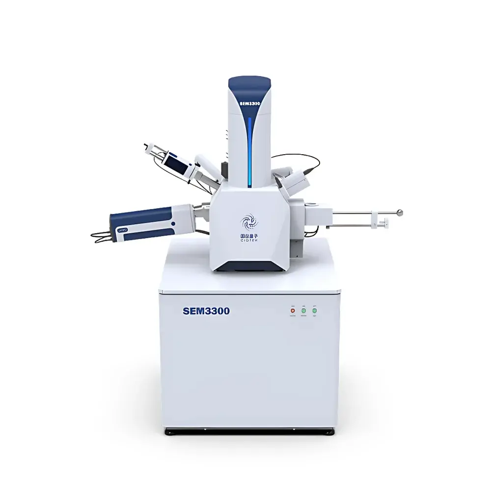
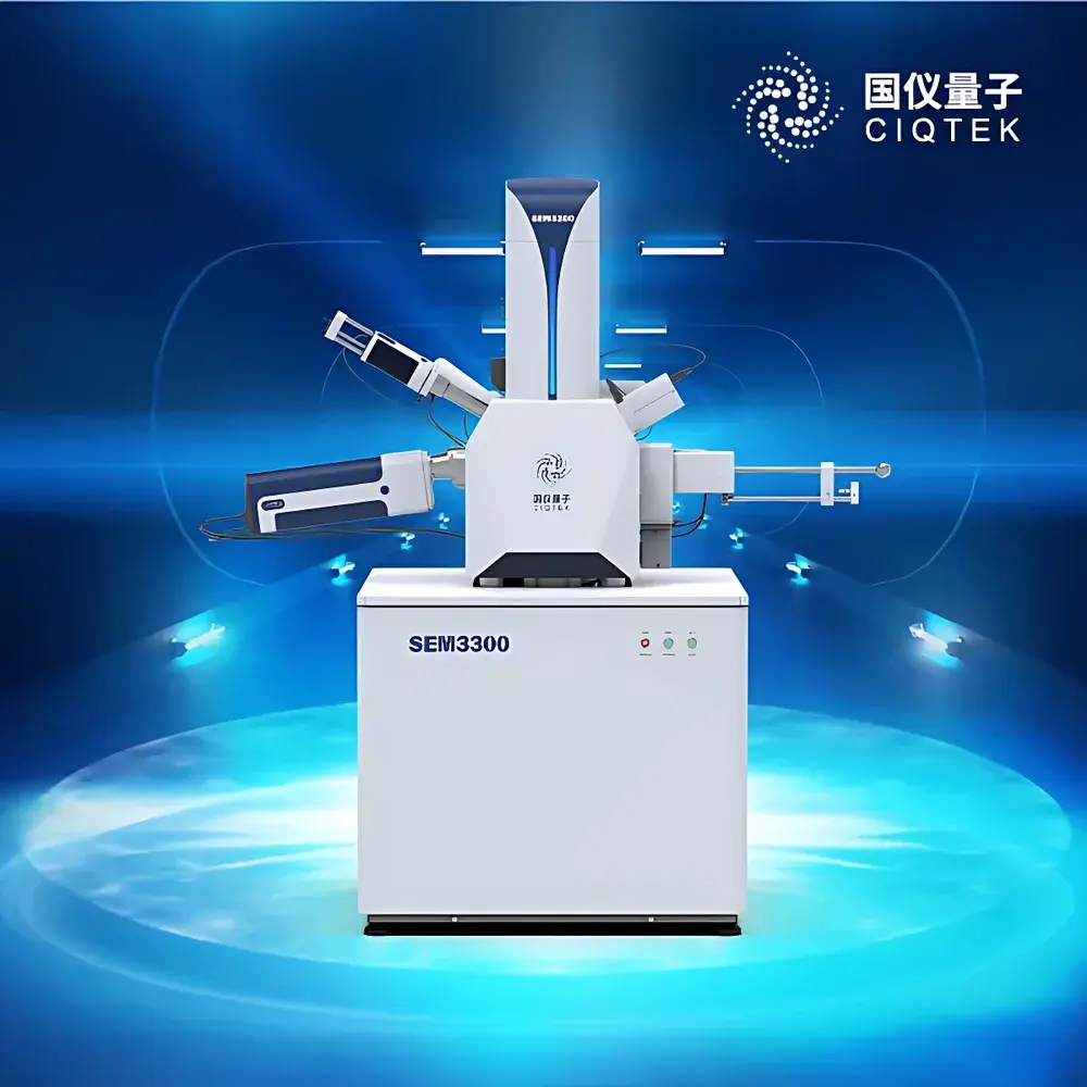
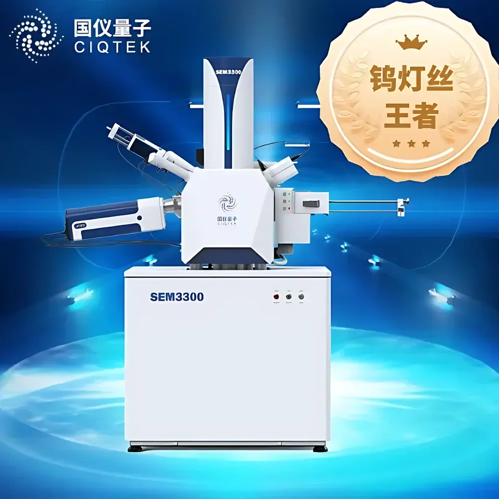
CIQTEK SEM3300 Tungsten-Filament Scanning Electron Microscope
| Brand | CIQTEK |
|---|---|
| Origin | Anhui, China |
| Manufacturer Type | Direct Manufacturer |
| Origin Category | Domestic (China) |
| Model | SEM3300 |
| Instrument Type | Floor-Standing Conventional SEM |
| Electron Source | Tungsten Filament |
| SEM Class | Entry-Level Tungsten-Filament SEM |
| Secondary Electron Resolution | 2.5 nm @ 20 kV |
| Magnification Range | 1× to 300,000× |
| Accelerating Voltage | 0.1 kV to 30 kV |
| Stage Travel | X: 120 mm |
| Y | 115 mm |
| Z | 50 mm |
Overview
The CIQTEK SEM3300 is a floor-standing tungsten-filament scanning electron microscope engineered for high-fidelity surface imaging in academic laboratories, quality control environments, and industrial R&D settings. Operating on the fundamental principle of raster-scanned electron beam interaction with solid specimens, the SEM3300 detects secondary electrons (SE) and backscattered electrons (BSE) to generate topographic and compositional contrast at sub-10 nm resolution. Its optimized electromagnetic lens column—featuring a multi-stage condenser system and high-stability final objective lens—enables consistent beam convergence across the full accelerating voltage range (0.1–30 kV). Unlike conventional tungsten-filament systems constrained by thermal emission limitations, the SEM3300 incorporates a proprietary electron optical path design that minimizes spherical and chromatic aberrations, thereby extending practical resolution performance into low-voltage regimes. At 1 kV, it achieves 5 nm SE resolution—a benchmark uncommon among entry-level tungsten sources—making it suitable for beam-sensitive, non-conductive, or nanostructured samples requiring minimal charging and reduced penetration depth.
Key Features
- High-resolution tungsten-filament source with extended lifetime and stable emission current (≥80 h typical at 30 kV)
- Multi-kV imaging capability: seamless transition from high-energy (30 kV) for deep material contrast to low-energy (0.1–3 kV) for surface-sensitive, charge-free imaging
- Large specimen chamber accommodating standard 100 mm diameter stubs and custom mounts up to 120 mm × 115 mm × 50 mm (X-Y-Z travel)
- Digital scan control with real-time frame averaging, drift compensation, and dynamic focus tracking
- Integrated vacuum system with turbo-molecular pump and ion getter pump, achieving base pressure ≤2 × 10⁻⁴ Pa in the specimen chamber
- Modular architecture supporting future upgrades including EDS detector integration, stage tilt/rotation, and cryo-transfer options
Sample Compatibility & Compliance
The SEM3300 accommodates a broad spectrum of conductive and non-conductive materials—including metals, ceramics, polymers, biological tissues (after sputter coating), geological sections, and nanomaterials—without compromising signal fidelity. Its low-voltage imaging mode (≤3 kV) significantly mitigates surface charging on insulators, reducing or eliminating the need for carbon/metal coating in many routine applications. The instrument complies with IEC 61000-6-3 (EMC emissions) and IEC 61000-6-2 (immunity), and meets CE safety directives (2014/35/EU Low Voltage Directive and 2014/30/EU EMC Directive). All operational parameters—including HV setting, magnification, working distance, and detector gain—are logged with timestamps for GLP/GMP-aligned documentation. Audit trail functionality supports traceability requirements under ISO/IEC 17025 and FDA 21 CFR Part 11 when paired with validated software configurations.
Software & Data Management
The SEM3300 operates via CIQTEK’s proprietary SEMControl Suite v3.x—a Windows-based platform built on Qt framework with deterministic real-time acquisition scheduling. It provides intuitive workflow navigation, customizable acquisition presets (e.g., “Polymer Low-kV”, “Metallography High-kV”), and synchronized multi-detector imaging (SE + BSE). Image metadata (including kV, WD, dwell time, pixel size, stage coordinates, and detector bias) are embedded in TIFF/DM3 file headers. Raw data export supports batch conversion to open formats (e.g., .tif, .png, .csv for intensity profiles). The software includes basic quantitative tools: particle analysis (size distribution, circularity, Feret diameter), line profile extraction, and grayscale histogram statistics. For regulated environments, optional validation packages include IQ/OQ documentation templates and electronic signature support compliant with ALCOA+ data integrity principles.
Applications
- Materials science: Fractography of alloys, grain boundary analysis in sintered ceramics, dispersion uniformity assessment of nanoparticle composites
- Electronics manufacturing: PCB trace inspection, solder joint morphology, MEMS device surface integrity verification
- Geosciences: Mineral phase identification (in conjunction with EDS), pore structure characterization in shale cores
- Life sciences: Coated biological specimens (e.g., pollen, diatoms, freeze-dried cells), biomaterial scaffold porosity mapping
- Quality assurance labs: Incoming raw material screening, failure root cause analysis (e.g., corrosion initiation sites, coating delamination)
FAQ
What is the typical filament lifetime under standard operating conditions?
Tungsten filaments operate reliably for ≥80 hours at 30 kV and ≥120 hours at 10 kV with recommended vacuum maintenance and proper warm-up protocols.
Can the SEM3300 be used without metal coating for non-conductive samples?
Yes—low-kV imaging (≤3 kV) combined with beam deceleration mode enables uncoated polymer, ceramic, and biological samples to be imaged with minimal charging artifacts.
Is remote operation supported?
The SEMControl Suite supports secure LAN-based remote access via VNC or RDP; however, live beam control requires local administrator privileges and hardware interlock verification.
Does the system meet regulatory requirements for pharmaceutical QC labs?
When deployed with validated software configuration, audit trail logging, and electronic signature modules, the SEM3300 satisfies core elements of USP <1058>, ASTM E2919, and ISO 13485 Annex A for analytical instrument qualification.
What vacuum level is required before initiating beam operation?
Beam emission is enabled only when chamber pressure reaches ≤2 × 10⁻⁴ Pa, verified by integrated Pirani + cold cathode gauges with automatic interlock enforcement.


