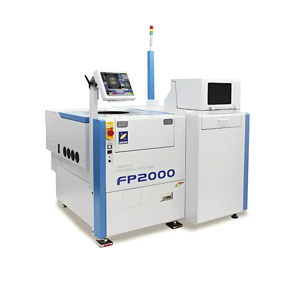
Accretech TSK FP-2000 Fully Automated Probe Station
| Brand | Accretech (ACCRETECH) |
|---|---|
| Origin | Japan |
| Model | FP-2000 |
| Operation Type | Fully Automatic |
| Maximum Wafer Size | 300 mm (12-inch) |
| Sample Types | Bare Wafers, Thin Wafers, Singulated Dies, CSP Substrates on Dicing Frames |
| Alignment Capability | Auto-Wafer Alignment, Auto-Probe-to-Pad Alignment, Die-Level Position Correction Software |
Overview
The Accretech TSK FP-2000 is a high-precision, fully automated probe station engineered for advanced semiconductor process development, wafer-level reliability testing, and characterization of front-end and back-end integrated circuit devices. Based on a rigid granite base and thermally stable mechanical architecture, the FP-2000 employs a motorized XYZθ stage with sub-micron repeatability and integrated vision-based alignment algorithms to ensure consistent electrical contact across high-density pad arrays. Its core measurement paradigm centers on low-noise, high-fidelity DC and RF parametric testing—enabling precise acquisition of IV, CV, pulsed IV, and S-parameter data under controlled environmental conditions. Designed specifically for 300 mm (12-inch) silicon wafers—including ultra-thin, warped, and dicing-frame-mounted CSP substrates—the system supports both front-side probing and optional backside illumination configurations for through-silicon via (TSV) and MEMS applications.
Key Features
- Fully automated wafer handling with robotic arm and cassette-to-chuck transfer—supports standard FOUPs, SMIF pods, and open cassettes
- Dual-vision system (top-view macro + high-magnification micro) with real-time image stitching and pattern recognition for die-level registration
- Proprietary die position correction software that compensates for wafer warpage, saw street distortion, and frame-induced substrate deformation
- Motorized probe card holder with fine Z-axis control (0.1 µm resolution) and automatic probe-to-pad touchdown detection
- Integrated thermal chuck with temperature range from −60 °C to +300 °C (optional liquid nitrogen or mechanical chiller support)
- Modular I/O interface supporting industry-standard protocols: GPIB, USB-TMC, Ethernet/IP, and SCPI-compliant command sets
- EMI-shielded enclosure compliant with SEMI S2/S8 safety and emissions requirements
Sample Compatibility & Compliance
The FP-2000 accommodates a broad spectrum of semiconductor substrates beyond standard 300 mm silicon wafers: thin wafers down to 50 µm thickness, temporary-bonded carrier wafers, laser-cut singulated dies, and fan-out wafer-level packages (FO-WLP) mounted on dicing frames. Its adaptive chuck design includes vacuum zoning and edge-clamp options to minimize stress-induced cracking during probing. The system conforms to key international standards for semiconductor equipment, including SEMI E10 (Definition of Equipment Reliability), SEMI E11 (Equipment Communication Standard), and ISO 9001:2015 certified manufacturing processes. For regulated environments, audit trails, user access levels, and electronic signature support align with FDA 21 CFR Part 11 and EU Annex 11 requirements when integrated with compliant test executive software.
Software & Data Management
The FP-2000 operates under Accretech’s proprietary ProStation Control Suite—a Windows-based platform supporting script-driven test sequencing, real-time data logging, and multi-instrument synchronization. The software features built-in statistical process control (SPC) modules, yield mapping visualization, and native export to CSV, Excel, and industry-standard STDF formats. All alignment routines, probe touchdown events, and environmental logs are timestamped and stored with SHA-256 hash integrity verification. Optional integration with Keysight PathWave, FormFactor Cascade Microtech Test Executive, or custom Python-based test frameworks is supported via standardized API libraries and DLL wrappers. Data retention policies, role-based permissions, and encrypted database backups meet GLP/GMP documentation integrity standards.
Applications
- Parametric testing of logic, memory, and analog ICs during process qualification and lot acceptance
- Reliability stress testing (HTOL, ESD, latch-up) at wafer level prior to packaging
- RF/mmWave device characterization up to 110 GHz using calibrated microwave probes and de-embedding capabilities
- Failure analysis site localization via synchronized optical beam-induced current (OBIC) and voltage contrast imaging
- Advanced packaging validation—including bump height uniformity, solder joint integrity, and redistribution layer (RDL) continuity checks
- Research-grade characterization of novel materials (GaN, SiC, 2D semiconductors) requiring low-force, high-resolution probing
FAQ
Does the FP-2000 support 200 mm and 150 mm wafers in addition to 300 mm?
Yes—the system is backward-compatible with smaller wafer sizes via configurable chuck inserts and updated recipe templates.
Can the FP-2000 be integrated with third-party parametric test systems (e.g., Keysight B1500A, Keithley 4200-SCS)?
Yes—standard SCPI command support and hardware trigger I/O enable seamless integration with major semiconductor test instrumentation platforms.
Is vacuum chucking available for fragile or low-k dielectric wafers?
Yes—multi-zone vacuum control and soft-landing algorithms minimize mechanical stress during chucking and probing cycles.
What level of positional accuracy does the auto-alignment system achieve?
Typical alignment repeatability is ≤ ±0.5 µm (3σ) under controlled lab conditions (23 ±1 °C, <45% RH), verified per ISO 20957-3 metrology guidelines.
Does the system include calibration certification and traceable documentation?
Each delivered FP-2000 includes NIST-traceable stage calibration reports, vision system MTF verification data, and factory alignment verification records compliant with ISO/IEC 17025.


