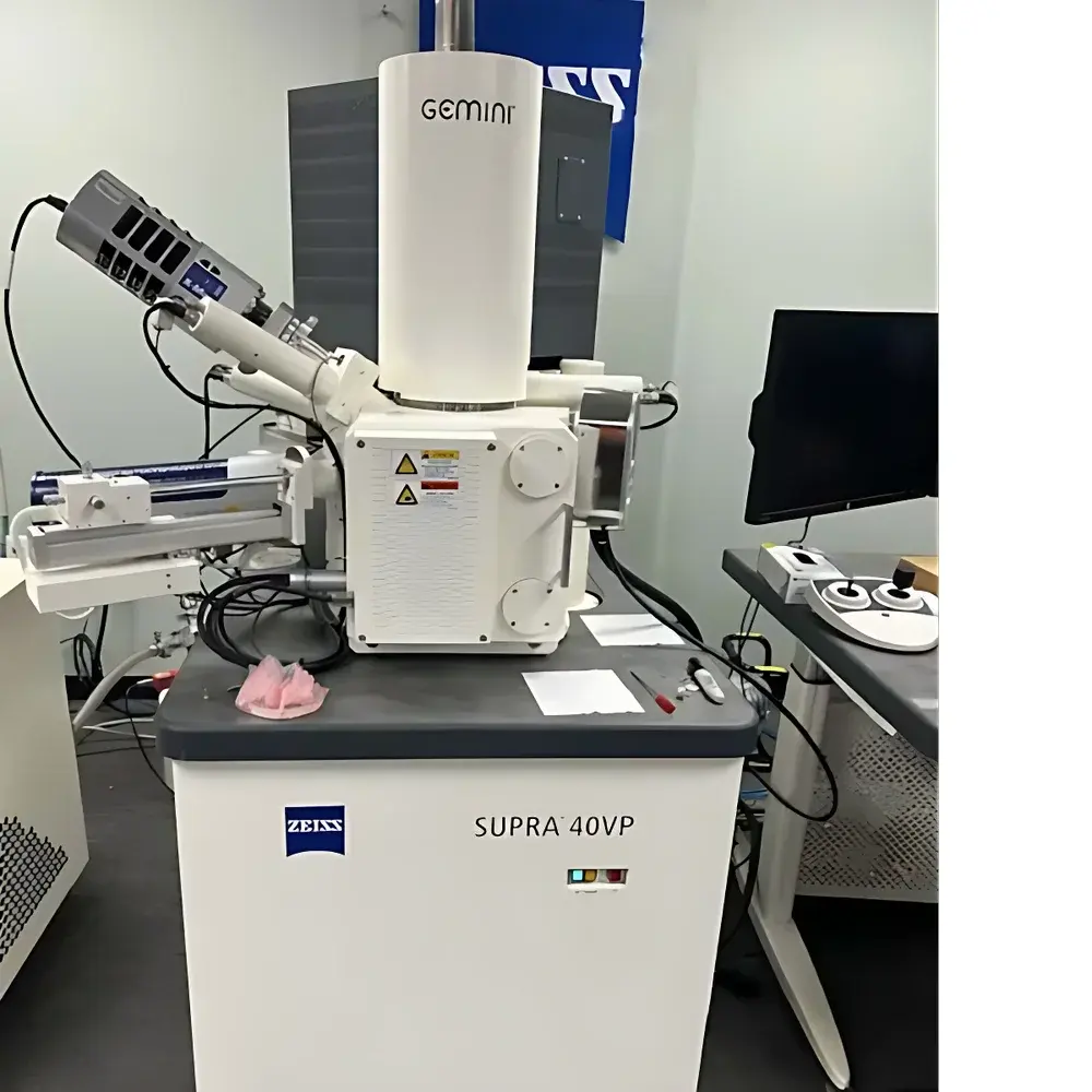
ZEISS SUPRA 40VP Field Emission Scanning Electron Microscope with Integrated Oxford EDS and EBSD Systems
| Brand | ZEISS |
|---|---|
| Origin | Germany |
| Configuration | SUPRA 40VP + Oxford X-MaxN EDS + Symmetry EBSD |
| Operating Hours | ~6 years |
| Resolution | 1.0 nm @ 20 kV (SE), 2.0 nm @ 30 kV (VP mode) |
| Acceleration Voltage | 0.1–30 kV |
| Vacuum Mode Range | 2–133 Pa (variable pressure, 1 Pa step) |
| Probe Current | 4 pA–10 nA (up to 20 nA optional) |
| Chamber Dimensions | Ø330 mm × H270 mm |
| Stage Motion | 5-axis motorized (X/Y ±130 mm, Z 0–50 mm, Tilt −3° to +70°) |
| Magnification | 12×–900,000× |
Overview
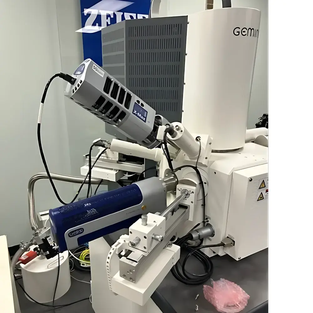
The ZEISS SUPRA 40VP is a high-performance field emission scanning electron microscope (FE-SEM) engineered for nanoscale imaging, microstructural characterization, and quantitative compositional analysis in demanding research and industrial environments. At its core lies the third-generation GEMINI electron optical column — a patented design featuring in-lens detection, aberration-optimized beam pathways, and active alignment compensation — delivering exceptional signal-to-noise ratio and sub-nanometer spatial resolution across a wide range of accelerating voltages (0.1–30 kV). Its variable pressure (VP) capability enables direct imaging of non-conductive or hydrated specimens without sputter coating, leveraging controlled gas injection (typically water vapor or nitrogen) to dissipate surface charge while preserving native morphology. Integrated Oxford Instruments hardware — including the X-MaxN silicon drift detector (SDD) for energy-dispersive X-ray spectroscopy (EDS) and the Symmetry CMOS-based electron backscatter diffraction (EBSD) system — transforms the platform into a comprehensive correlative microscopy solution for phase identification, crystallographic orientation mapping, grain boundary analysis, and strain evaluation at the micron-to-submicron scale.
Key Features
- GEMINI II column architecture with cold field emission source (CFEG), enabling stable high-brightness probe formation and long-term beam coherence
- Variable pressure mode (2–133 Pa, adjustable in 1 Pa increments) with differential pumping and environmental SE/BSE detectors for uncoated insulator imaging
- Large-volume sample chamber (Ø330 mm × 270 mm height) accommodating multi-detector configurations and extended-stage accessories
- Motorized 5-axis precision stage (X/Y ±130 mm, Z 0–50 mm, tilt −3° to +70°, rotation 360°) supporting automated serial sectioning and tilt-series acquisition
- Oxford X-MaxN 80 mm² SDD EDS system with ultra-thin window, <123 eV Mn-Kα resolution, and real-time spectrum imaging (SI) processing
- Oxford Symmetry EBSD detector with 16-bit CMOS sensor, >100 fps pattern acquisition, and integrated AZtecCrystal software for orientation mapping, phase discrimination, and misorientation analysis
- Integrated SmartSEM software suite with scripting support (Python API), batch acquisition workflows, and GLP-compliant metadata tagging
Sample Compatibility & Compliance
The SUPRA 40VP accommodates diverse specimen geometries — from bulk metallic alloys and ceramic composites to geological thin sections, polymer blends, biological tissues (critical-point dried or cryo-prepared), and semiconductor wafers up to 200 mm diameter. Its VP mode eliminates charging artifacts on polymers, ceramics, and biological materials, while low-kV imaging (<5 kV) preserves surface topography and minimizes beam damage. The system complies with IEC 61000-6-3 (EMC), IEC 61000-6-4 (industrial immunity), and meets CE safety requirements. All EDS/EBSD data acquisition and reporting modules support audit trail functionality per FDA 21 CFR Part 11 when deployed in regulated QA/QC laboratories. Routine operation adheres to ASTM E1508 (quantitative EDS microanalysis) and ASTM E2627 (EBSD pattern indexing standards).
Software & Data Management
Acquisition, processing, and reporting are unified under ZEISS SmartSEM v7.x and Oxford AZtec 4.x platforms. SmartSEM provides intuitive workflow-driven control of SEM parameters, stage navigation, and multi-signal synchronization (SE, BSE, EDS, EBSD). AZtec integrates live EDS spectrum imaging with EBSD orientation maps, enabling simultaneous chemical and crystallographic correlation. Data files (.smv, .h5, .azd) are stored with embedded calibration metadata, instrument configuration logs, and user-defined annotations. Export options include TIFF, CSV, HDF5, and OIM Analysis-compatible formats. Networked deployment supports centralized license management, remote diagnostics, and secure data transfer via TLS-encrypted FTP/SFTP — essential for multi-user academic cores and contract testing facilities.
Applications
- Materials science: Grain size distribution, twin boundary analysis, texture evolution in deformation studies, intermetallic phase identification
- Failure analysis: Fracture surface characterization, inclusion mapping, corrosion product phase differentiation, solder joint voiding assessment
- Nanotechnology: Nanoparticle dispersion homogeneity, carbon nanotube alignment quantification, quantum dot crystallinity verification
- Geosciences: Mineral phase assemblage mapping, porosity-permeability correlation in reservoir rocks, metamorphic reaction rim analysis
- Electronics: Cross-sectional interface analysis, Cu diffusion profiling in BEOL stacks, solder bump intermetallic compound (IMC) growth kinetics
- Life sciences: Cell membrane topology, collagen fibril orientation in decellularized scaffolds, nanoparticle internalization pathways in fixed tissue
FAQ
Is this instrument fully refurbished and warranted?
Yes — this unit underwent full OEM-level refurbishment by a ZEISS-certified service partner, including column bake-out, detector recalibration, vacuum system validation, and software reinstallation. A 12-month parts-and-labor warranty is included.
Does it support automated EBSD phase identification?
Yes — AZtec Crystal includes a built-in phase library manager and supports automated indexing against ICDD PDF-4+ and custom crystal structure databases (CIF format), with confidence index filtering and pattern quality optimization.
Can the system be upgraded to support FIB-SEM integration?
The mechanical and electrical interfaces of the SUPRA 40VP chamber are compatible with select ZEISS CrossBeam systems; however, retrofitting requires factory engineering review and additional vacuum interlock modifications.
What documentation accompanies the system?
Full delivery includes original ZEISS technical manuals, Oxford EDS/EBSD installation certificates, calibration reports (resolution, energy scale, pattern center), and a traceable maintenance history log.
Is remote training and application support available post-installation?
Yes — ZEISS and Oxford jointly provide 20 hours of virtual application support, including method development for specific sample types, EDS quantification standardization, and EBSD map post-processing workflows.


")
