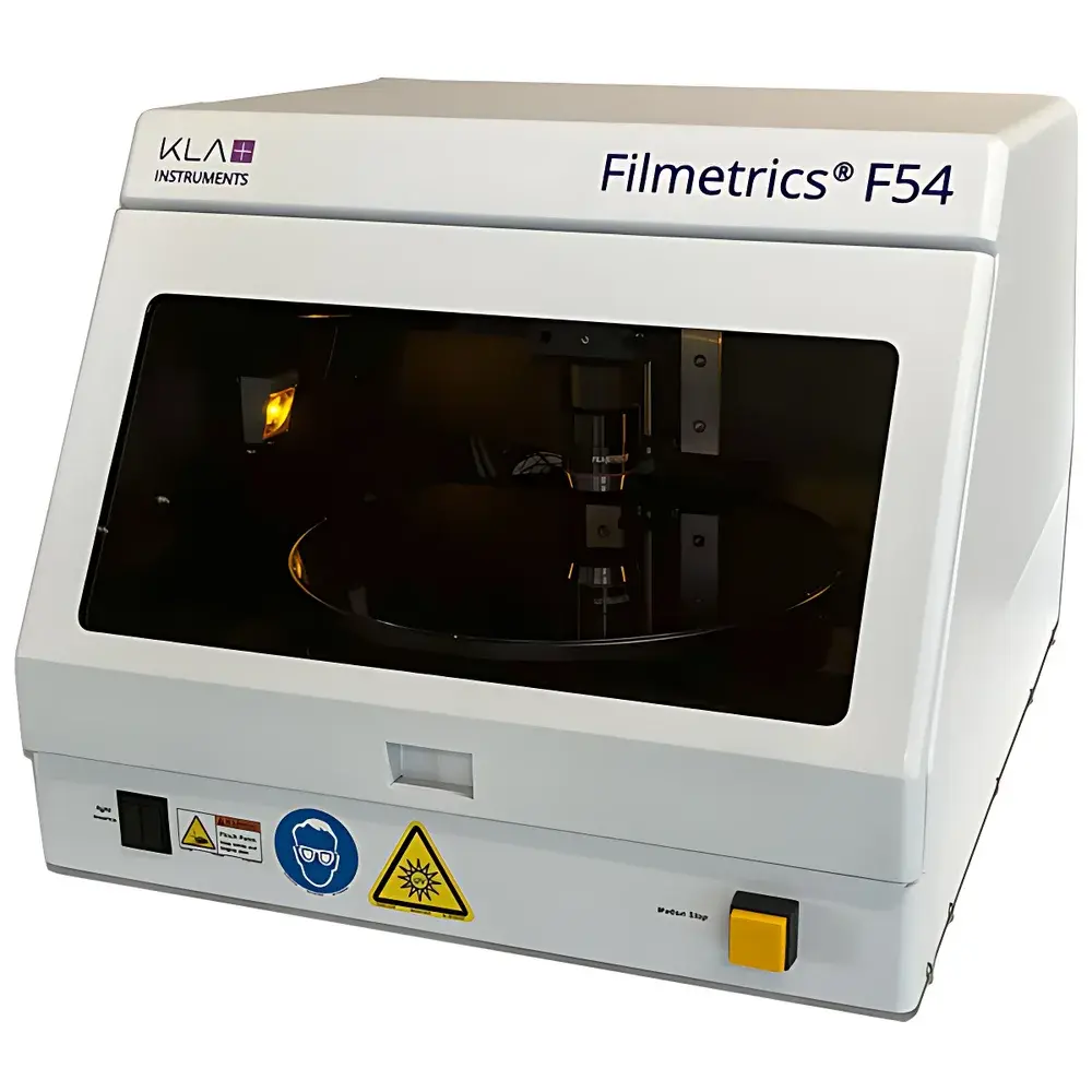
KLA Filmetrics F54-XY Series White Light Interferometric Thin-Film Thickness Metrology System
| Brand | KLA |
|---|---|
| Origin | USA |
| Manufacturer | KLA Corporation |
| Product Type | Imported Instrument |
| Model | F54-XY Series |
| Pricing | Upon Request |
| Thickness Range (F54-XY) | 20 nm – 50 µm |
| Wavelength Range (F54-XY) | 380–1050 nm |
| Thickness Range (F54-XY-UV) | 4 nm – 35 µm |
| Wavelength Range (F54-XY-UV) | 190–1100 nm |
| Thickness Range (F54-XY-NIR) | 100 nm – 120 µm |
| Wavelength Range (F54-XY-NIR) | 950–1700 nm |
| Thickness Range (F54-XY-EXR) | 20 nm – 120 µm |
| Wavelength Range (F54-XY-EXR) | 380–1700 nm |
| Thickness Range (F54-XY-UVX) | 4 nm – 120 µm |
| Wavelength Range (F54-XY-UVX) | 190–1700 nm |
| Maximum Sample Size (F54-XY-200) | 200 mm |
| Maximum Sample Size (F54-XYT-300) | 300 mm |
| Measurement Speed | Up to 2 fields of view per second |
| Stage Type | Motorized XY stage (F54-XY-200) |
| Pattern Recognition | Yes, supports both arrayed and non-arrayed wafers |
| Software | FILMapper v6.x or later |
| Compliance | NIST-traceable calibration standards included |
| Material Library | >130 built-in optical constants |
Overview
The KLA Filmetrics F54-XY Series is a high-precision, white light interferometric thin-film thickness metrology system engineered for automated, non-contact, and non-destructive measurement of single- and multi-layer films on patterned and unpatterned semiconductor wafers. Based on spectral reflectance analysis, the system captures interference fringes generated at film-substrate and film-air interfaces across a broad spectral range—enabling accurate determination of optical thickness (n·t), where n is refractive index and t is physical thickness. Unlike stylus profilometry or ellipsometry, white light interferometry offers rapid, wide-area mapping without requiring vacuum environments or complex alignment. The F54-XY platform integrates a modular spectrometer, broadband illumination optics, and a motorized precision stage to support full-wafer characterization up to 300 mm in diameter, with sub-nanometer resolution in thickness and <0.3% repeatability under controlled environmental conditions.
Key Features
- Modular optical architecture supporting five wavelength configurations: UV (190–1100 nm), VIS-NIR (380–1050 nm), NIR (950–1700 nm), extended-range EXR (380–1700 nm), and UVX (190–1700 nm)—optimized for diverse film types including SiO₂, SiNₓ, photoresists, metals, polymers, and transparent conductive oxides.
- Motorized XY translation stage (F54-XY-200) or combined XY + rotation stage (F54-XYT-300) enabling programmable point selection across wafer surfaces using rectangular, polar, linear, or user-defined coordinate arrays—no hard limit on number of measurement points.
- Onboard pattern recognition engine that automatically identifies die locations, scribe lanes, and feature edges—eliminating manual registration for both regular array layouts and irregularly patterned substrates.
- FILMapper software suite providing real-time spectral fitting, multi-layer modeling (up to 5 layers), dispersion correction via Cauchy or Sellmeier models, and batch processing with CSV/PDF export.
- Factory-calibrated with NIST-traceable SiO₂ and silicon reference standards; includes integrated vacuum pump for chuck-based sample holding and optional high-pass filter wheel for spectral noise suppression.
Sample Compatibility & Compliance
The F54-XY series accommodates rigid planar substrates ranging from 50 mm to 300 mm in diameter—including silicon, sapphire, glass, and compound semiconductor wafers—with or without microstructures, trenches, or embedded metallization. It supports opaque, semi-transparent, and highly absorbing films, as well as rough surfaces (Ra < 100 nm) when paired with appropriate averaging protocols. All systems ship with ISO/IEC 17025-aligned calibration documentation and comply with ASTM F398 (Standard Practice for Spectral Reflectance Measurements of Thin Films) and SEMI E152 (Specification for Optical Thin Film Thickness Measurement Systems). Optional audit trail logging and electronic signature modules enable compliance with FDA 21 CFR Part 11 and GLP/GMP quality systems.
Software & Data Management
FILMapper v6.x provides a unified interface for instrument control, data acquisition, model building, and reporting. Its scripting API (Python-compatible) enables integration into factory automation frameworks such as SECS/GEM. Measurement data are stored in hierarchical HDF5 format, preserving raw spectra, fit parameters, metadata (timestamp, operator ID, stage coordinates), and uncertainty estimates. Built-in statistical process control (SPC) tools generate X-bar/R charts, Cp/Cpk reports, and spatial heatmaps overlaid directly onto wafer layout diagrams. All software updates, application notes, and remote diagnostic support are accessible via secure HTTPS connection—requiring no local server infrastructure.
Applications
- Front-end semiconductor process control: monitoring gate oxide uniformity, ARC layer thickness, and CMP endpoint detection on 200 mm and 300 mm wafers.
- MEMS and advanced packaging: measuring passivation layers (e.g., SiNₓ), redistribution layers (RDLs), and under-bump metallization (UBM) stacks.
- Display manufacturing: quantifying ITO, MoO₃, and organic emissive layer thicknesses on TFT backplanes and flexible substrates.
- R&D laboratories: characterizing novel 2D materials (MoS₂, h-BN), perovskite photovoltaic layers, and ALD-grown ultra-thin films down to 4 nm.
- Quality assurance in optical coating facilities: verifying quarter-wave stacks, anti-reflective coatings, and laser mirror designs.
FAQ
What film thickness ranges does the F54-XY support?
Depending on configuration, the system measures films from 4 nm (UVX mode) to 120 µm (NIR/EXR modes), with optimal accuracy achieved within ±5% of nominal thickness when optical constants are known or calibrated.
Can the F54-XY measure multi-layer stacks?
Yes—FILMapper supports simultaneous fitting of up to five layers using physically constrained optical models, including graded interfaces and dispersion-corrected refractive indices.
Is the system compatible with cleanroom environments?
All F54-XY variants meet ISO Class 5 particulate requirements when operated with standard HEPA-filtered air handling; optional nitrogen purge kits are available for Class 1 compatibility.
How is traceability ensured for production measurements?
Each system includes NIST-traceable SiO₂ thickness standards and certified silicon reflectance references; calibration certificates list measurement uncertainty budgets per ISO/IEC 17025 Annex A.
Does the software support automated recipe transfer across multiple tools?
Yes—FILMapper uses XML-based recipe files that retain all optical models, stage maps, and pass/fail criteria, enabling seamless deployment across fab-wide metrology networks.


