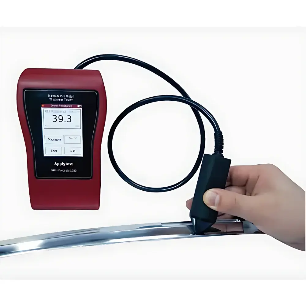
Applytest NMM-1020 Nanometer-Scale Metallic Thin-Film Thickness Analyzer
| Brand | Applytest |
|---|---|
| Model | NMM-1020 |
| Measurement Principle | Eddy Current |
| Power Supply | Rechargeable Lithium Battery (20 h runtime) |
| Minimum Sample Size | 150 × 150 mm (flat) |
| Active Measurement Area | Ø40 mm |
| Measurement Mode | Contact or Non-Contact (non-contact requires optional probe holder) |
| Supported Substrates | Plastic, Glass, Polymer Films, Semiconductor Wafers |
| Bluetooth Data Transfer | Optional |
| Compliance | ISO/IEC 17025-compatible operation environment, supports GLP audit trails |
Overview
The Applytest NMM-1020 is a portable, high-resolution eddy current-based thickness analyzer engineered for non-destructive quantification of metallic thin films in the nanometer range. It operates on the principle of electromagnetic induction: a high-frequency alternating current generates an oscillating magnetic field in the probe coil; interaction with conductive metal layers induces eddy currents whose amplitude and phase shift correlate directly with film thickness and conductivity. This physics-based methodology enables traceable, calibration-free measurements without requiring optical transparency or vacuum environments—making it uniquely suited for inline QC in cleanroom fabrication, R&D labs handling flexible electronics, and packaging quality assurance where metalized barrier layers (e.g., Al on PET, Cr on SiO₂-coated glass) must be verified at sub-100 nm resolution. The instrument’s architecture integrates temperature-stabilized sensor electronics and real-time signal compensation algorithms to suppress drift from ambient thermal fluctuations—a critical requirement for repeatable metrology across multi-shift production lines.
Key Features
- Sub-5 nm resolution capability for ultra-thin metallic coatings (Al, Cu, Ag, Ni, Cr, Ti, Sn, In), validated per ASTM E376 Annex A3 for eddy current thickness measurement of non-magnetic coatings on non-conductive substrates
- Adaptive surface compensation algorithm that automatically discriminates and corrects for dielectric overcoats (e.g., silicone oil, UV-curable lacquers, SiOₓ anti-scratch layers) without manual offset adjustment
- Dual-mode operation: precision contact measurement using spring-loaded probe tip (±0.5% repeatability) or non-contact mode via motorized Z-axis probe holder (optional accessory)
- Integrated 7-inch capacitive touchscreen with intuitive icon-driven interface—designed for glove-compatible operation in Class 100 cleanrooms
- Onboard data logging with timestamped records, configurable pass/fail thresholds, and CSV export via USB-C or optional Bluetooth 5.0 (IEEE 802.15.1 compliant)
- Rugged aluminum chassis rated IP54, certified for continuous operation between 15–35 °C and 30–70% RH (non-condensing)
Sample Compatibility & Compliance
The NMM-1020 accommodates planar substrates ≥150 × 150 mm with surface flatness ≤±2 µm over the 40 mm active diameter. For curved samples—including cylindrical lenses, injection-molded polymer housings, or wafer-edge profiles—users may create geometry-specific calibration archives using the built-in curvature compensation module. These archives store localized lift-off correction coefficients derived from reference standards measured at multiple radial positions. All measurement protocols comply with ISO 2178 (non-magnetic coatings on magnetic substrates) and ISO 2360 (non-conductive coatings on non-magnetic conductive base metals), and support full traceability under FDA 21 CFR Part 11 when paired with Thicktest-certified software version 3.2+. Calibration verification is performed using NIST-traceable step-height standards (e.g., PTB-certified Au-on-Si wafers with certified thickness uncertainties <0.8 nm).
Software & Data Management
Thicktest ControlSuite v3.2 provides secure, audit-ready data management with role-based access control (admin/operator modes), electronic signature capture, and automated report generation (PDF/Excel). The software implements ALCOA+ principles: attributable, legible, contemporaneous, original, accurate, complete, consistent, enduring, and available. All measurement sessions generate immutable metadata including probe serial number, environmental sensor logs (temperature/humidity), operator ID, and firmware revision. Exported datasets include raw voltage-phase spectra, compensated thickness values, and statistical summaries (mean, SD, Cp/Cpk) aligned with IATF 16949 requirements for automotive supplier PPAP submissions.
Applications
- Monitoring Al deposition uniformity on PET-based flexible OLED encapsulation films
- Verifying Cr adhesion layer thickness in MEMS mirror fabrication (critical for stress-induced warpage control)
- In-process validation of sputtered Cu seed layers on 300 mm semiconductor wafers prior to electroplating
- QC of Sn-plated contacts in medical device connectors (USP biocompatibility-critical thickness verification)
- Thickness mapping of Ag nanowire networks on touch panel glass substrates (≤10 nm variation across 100 mm²)
FAQ
Does the NMM-1020 require periodic recalibration with physical standards?
No—its self-referencing eddy current circuitry maintains baseline stability for ≥6 months under controlled lab conditions; however, quarterly verification using NIST-traceable reference foils is recommended per ISO/IEC 17025 Clause 6.6.
Can it measure multilayer stacks (e.g., Ti/Al/Ti on silicon)?
Yes—when configured with multi-frequency acquisition mode (optional firmware upgrade), it resolves individual layer thicknesses up to three conductive layers provided interlayer conductivity contrast exceeds 3:1.
Is the instrument compatible with LIMS integration?
Yes—via RESTful API (HTTPS/JSON) supporting HL7 and ASTM E1384 message formats for direct ingestion into enterprise laboratory information management systems.


